
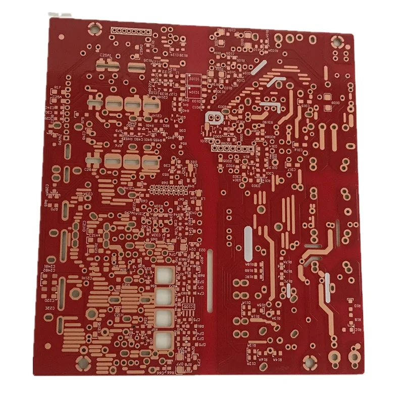
32 Gang Network WiFi TCP IP Relay Control Diy Switch Module PCB Board Smart Home Automation Remote Security Alarm Domotica
- Category: >>>
- Supplier: Qimao Electronics (Dingnan) Co. Ltd.
Share on (1600075613625):
Product Overview
Description
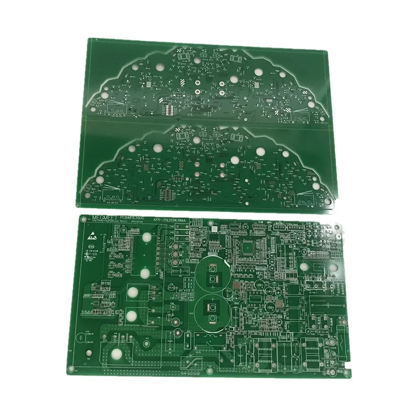
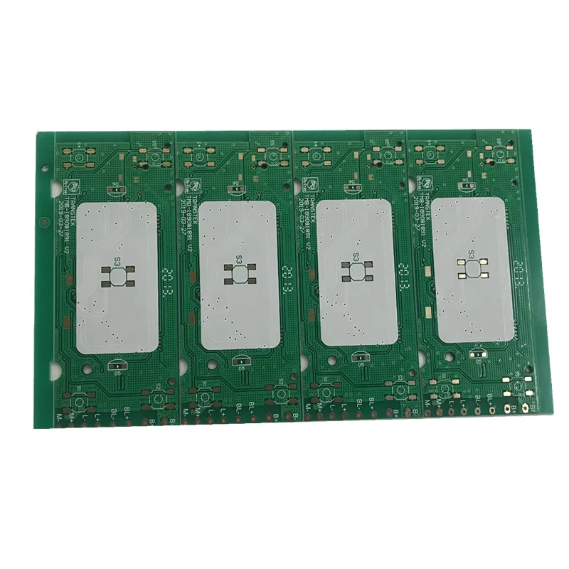
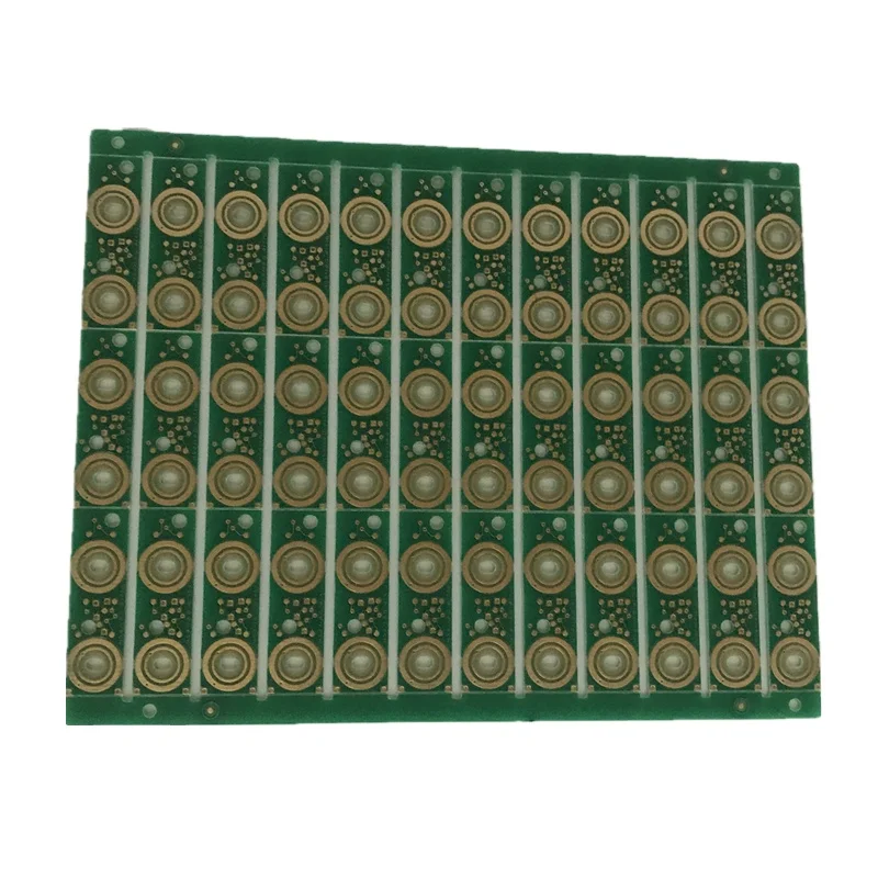
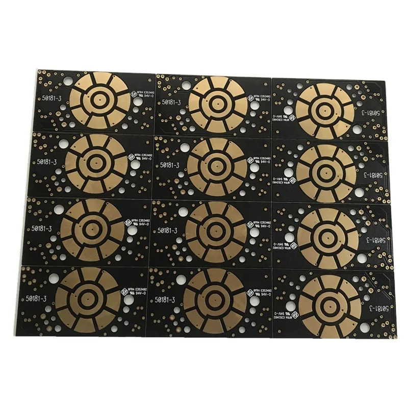
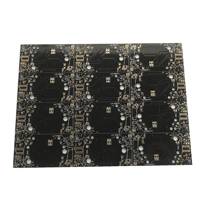
Product Description


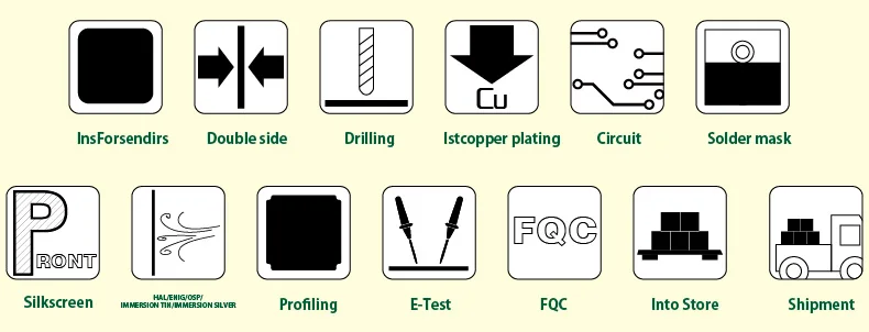
Packaging & Shipping
| ITEMS | Parameter | Remarks | |||||||||||
| Double side & Multi-layer | |||||||||||||
| Number of Layers | 1-20 layers | ||||||||||||
| Board Materials | FR4,CME3,CME1,5G | ||||||||||||
| PCB Size (Min- Max) | 50x80mm to 1000mm×600mm ( 39.37"x23.6") | ||||||||||||
| innerlayer line width/space(min) | 4mil/4mil(100um/100um) | ||||||||||||
| Finish Plating /Surface Finishes | HASL ,OSP,ENIG,HASL,gold finger,Au Panel,OSP,ENIG | ||||||||||||
| innerlayer pad (min) | 5mil(0.13mm) | Pad annular | |||||||||||
| Core thickness (min) | 8mli(0.2mm) | ||||||||||||
| Finisher Copper Inner Layers | 1/2oz(17um)a- | No Cu Clad | |||||||||||
| Finished Copper Outer Layers | 1/2oz(17um) | ||||||||||||
| Final PCB Thickness (tolerance %) | 0.5-4.0mm | ||||||||||||
| Final PCB Thickness (tolerance %) | Thickness<1.0mm | ||||||||||||
| 1.0mm≤Thickness<2.0mm | |||||||||||||
| Thickness≥2.0mm | |||||||||||||
| inner layer process | Brown Oxide | ||||||||||||
| Minimum Conductor Space | ±3mil(±76um) | ||||||||||||
| Minimum Drill Hole Size | 0.25mm | ||||||||||||
| min diameter of finished hole | 0.2mm | ||||||||||||
| Hole position accuracy | ±2mil(±50um) | ||||||||||||
| Drilled slot tolerance | ±3mil(±75um) | ||||||||||||
| PTH tolerance | ±2mil(±50um) | ||||||||||||
| NPTH tolerance | ±1mil(±25um) | ||||||||||||
| maxA.R.Of PTH | 08:01 | ||||||||||||
| PTH hole copper thickness | 0.4-2mil(10-50um) | ||||||||||||
| image to image tolerance | ±3mil(0.075mm) | ||||||||||||
| outer layer line width/space(min) 3mil/3mil(75um/75um) | |||||||||||||
| Solder Mask Thickness | line end 0.4-1.2mil(10-30um) | ||||||||||||
| line Corner ≥0.2mil(5um) | |||||||||||||
| on Substrate | ≤Finished Cu | ||||||||||||
| thickness+1.2mm≤Finished Cu | |||||||||||||
| thickness+30um)≤+1.2mil≤+30um) | |||||||||||||
| min solder mask dam | 4.0mil(100um) | ||||||||||||
| impedance control and tolerance 50Ω±10% | |||||||||||||
| warp and twist | ≤0.5% | ||||||||||||
| Delivery time | 1-2 layers 10-12day | ||||||||||||
| 4-20 layers 12-20days | |||||||||||||
| Package | General export packaging | ||||||||||||
technological

About us

Certifications

FAQ
Q:Are you manufacturer or trading company?
A: We are Manufacturer located in Jiangxi Ganzhou China. Specialized in manufacturing double-panel and multi-board PCB for over 18 years
Q:How long is your delivery time?
A:Samples need 3-5 working days,Mass production need 7-10 working days.
Q:Do you provide samples? Is it free or extra?
A: Yes,we offer the sample for free if we have it in stock.But need you pay the express fee.
Q: What is your payment terms?
A: Payment term is full payment if an trial order. And bulk order is 50% deposit and balance50% before delivery.
Q: What is your payment ways?
A: TT /Western union/ Paypal/Credit card etc.
Q:What express can we choose?
A:FedEx, UPS, DHL,TNT etc.
Q: What is you MOQ?
A: Our MOQ is 5 PANEL.
Q:Which files will need for produce PCB?
A: All pcb boards are OEM design,Send us PCB design(gerber,DXP,99SE file all ok for us)
Q:Is safty for my PCB design for manufacturing?
A: All customer's copyright will never manufacture PCB board for someone else with your files unless we receive written.
We Recommend
New Arrivals
New products from manufacturers at wholesale prices


