
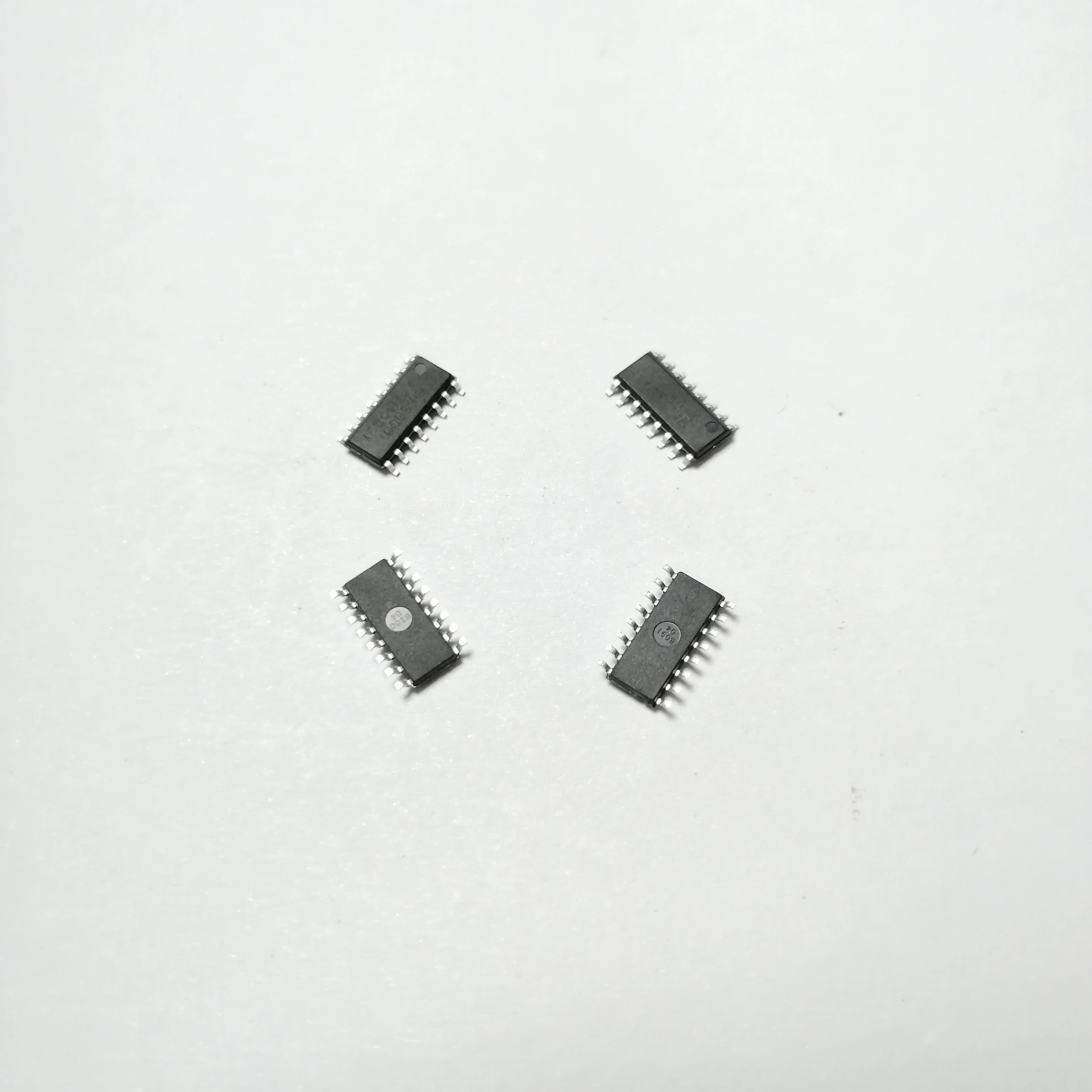
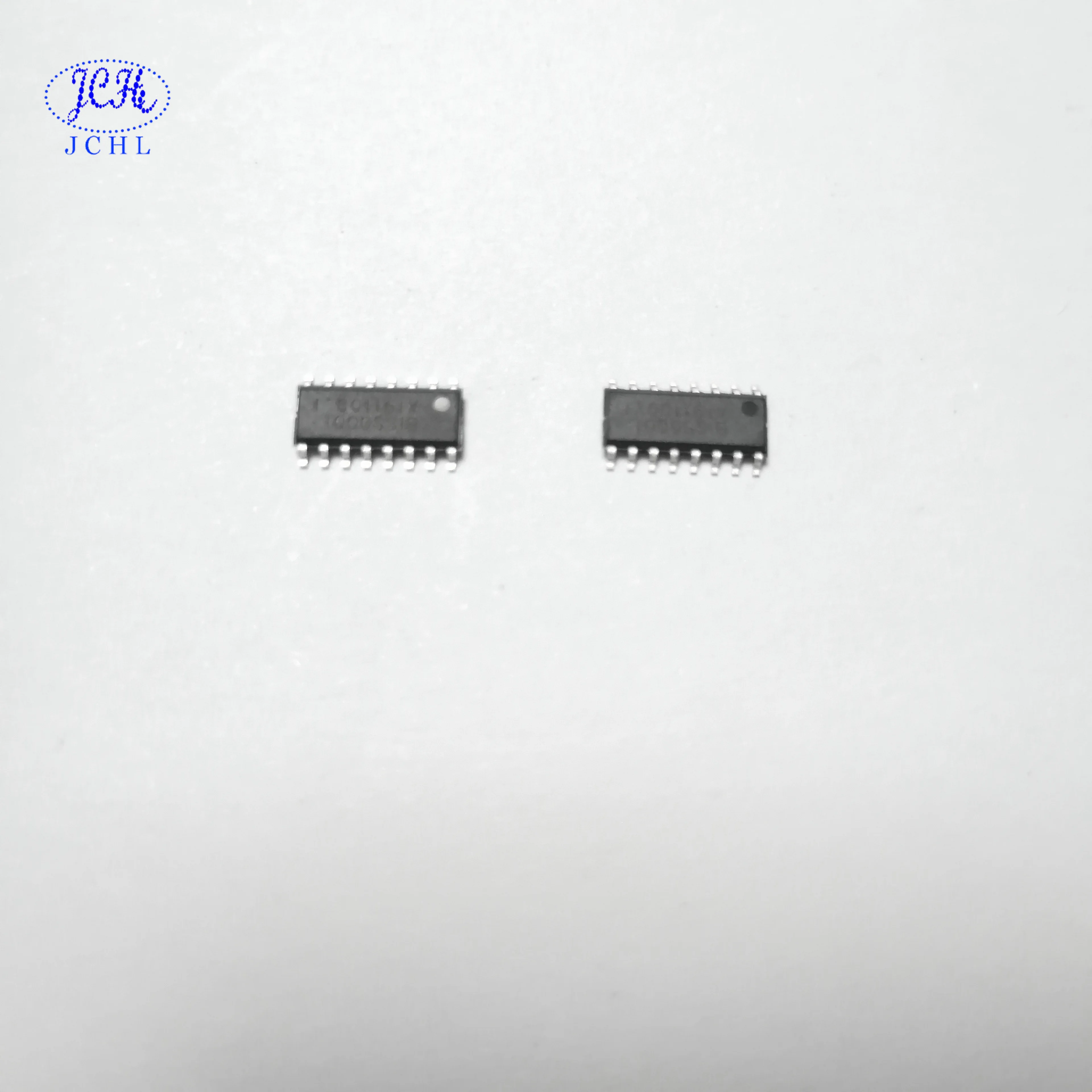
SOP16 package/Hybrid digital and analog processing/BISS0001 chip which designed for infrared sensors
- Category: >>>
- Supplier: Shenzhen Jingchuangheili Technology Co. Ltd.
Share on (1600079483790):
Product Overview
Description
Product Description
The BISS0001 is a hybrid digital and analog processing chips which designed for infrared sensor applications.
BISS0001 adopts the packaging form of SOP16. Only a few SMT components are needed for the peripheral application circuit, and no external voltage stabilizing circuit is needed, which greatly simplifies the peripheral circuit, saves PCB space, and reduces the overall BOM cost.
Features:
1,Low power CMOS technology (ider for battery operated PIR decices)
2,CMOS high input impedance operational amplifiers
3,Bi-directional level detector / Excellent noise immunity
4,Built-in Power up disable & output pulse control logic
5,Dual mode:retriggerable & non-retriggerable
Lighting control, motor and solenoid valve control, burglar alarm and other fields

Pin description:
Pin Number | Symbol | Description |
1 | A | Retriggerable & non-retriggerable mode select(A=1:re-triggerable) |
2 | VO | Detector output pin (active high) |
3 | RR1 | Output pulse width control (TX) * See definition below |
4 | RC1 | Output pulse width control (TX) * |
5 | RC2 | Trigger inhibit control (Ti) * |
6 | RR2 | Trigger inhibit control (Ti) * |
7 | Vss | Ground |
8 | VRF | RESET & voltage reference input (Normally high. Low=reset) |
9 | VC | Trigger disable input (VC>0.2 Vdd=enable; VC<0.2 Vdd=disabled |
10 | IB | Op-amp input bias current setting |
11 | Vdd | Supply voltage |
12 | 2OUT | 2nd stage Op-amp output |
13 | 2IN- | 2nd stage Op-amp inverting input |
14 | 1IN+ | 1 st stage Op-amp non-inverting input |
15 | 1IN- | 1 st stage Op-amp inverting input |
16 | 1OUT | 1 st stage Op-amp output |
*
Tx = The time duration during which the output pin (Vo) remains high after triggering.
Ti = During this time period,triggering is inhibited. See timing charts for details.
Absolute max. ratings
Description | Condition | Range | Unit |
Supply voltage | -- | 3~5 | V |
Input voltage | -- | Vss-0.3~Vdd+0.3 | V |
Output current | Vdd=5V | 10 | mA |
Operating temperature | -- | -20~+70 | ℃ |
Storage temperature | -- | -40~+125 | ℃ |

Application circuit example
More products

Supply Ability
Supply Ability:100000 pieces / per week
Applications in life


About us

Our Advantages


Package & Shipment

FAQ


We Recommend

New Arrivals
New products from manufacturers at wholesale prices


