
PCBA Electronic Assembly PCB Design Services PCB manufacturers
- Category: >>>
- Supplier: Dalian Jinseo Electronic Technology Co. Ltd.
Share on (1600364573904):
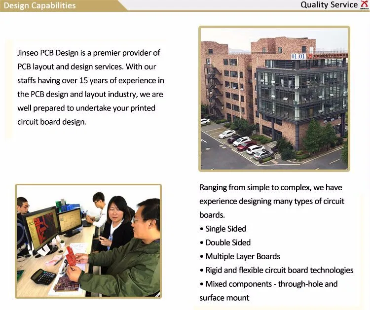
Product Overview
Description
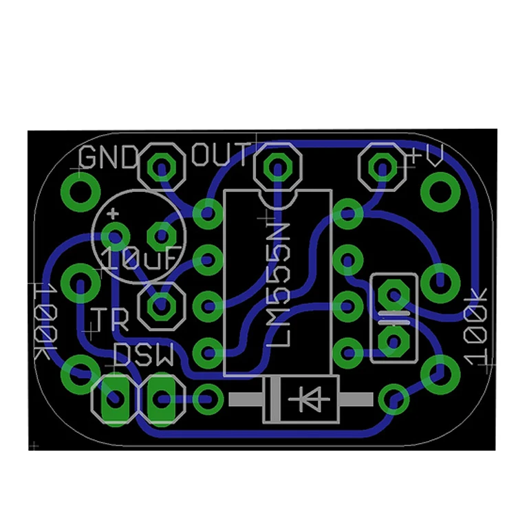
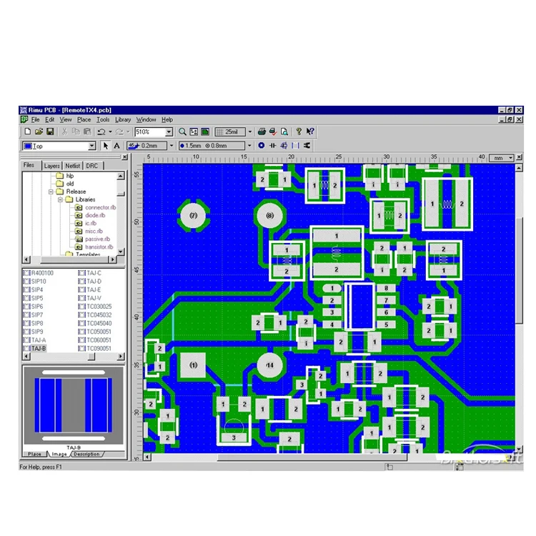
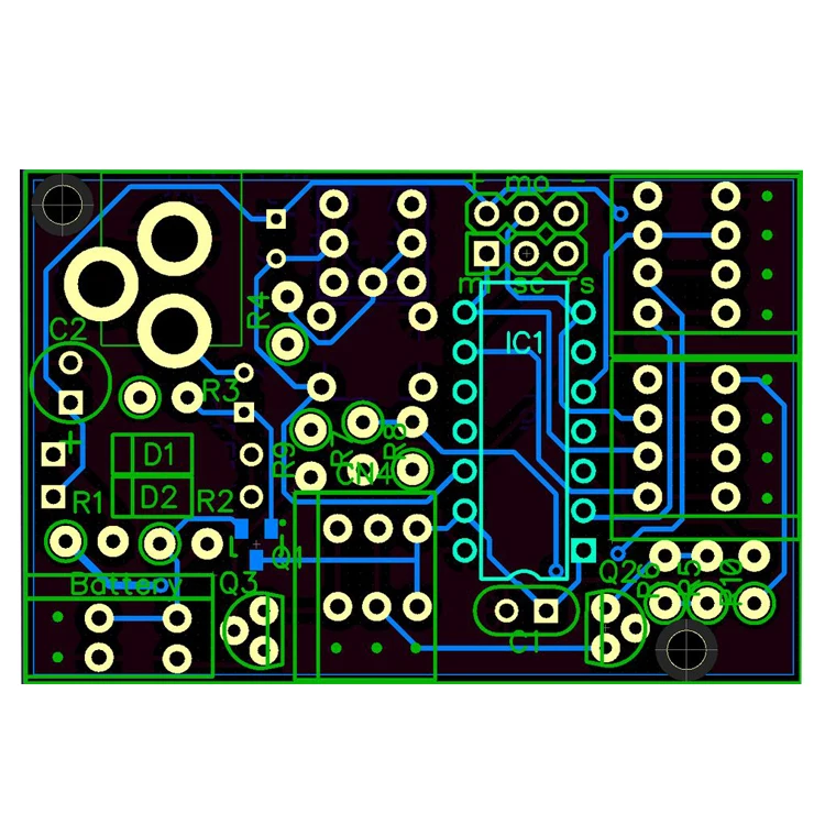
pcb design


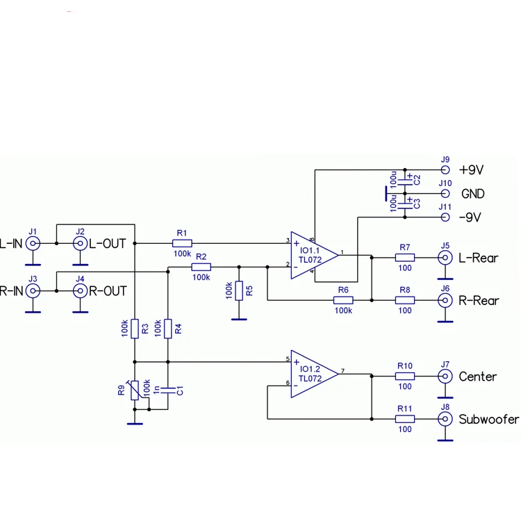
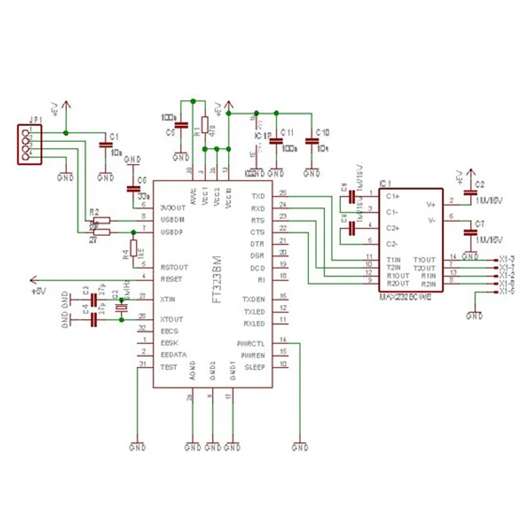
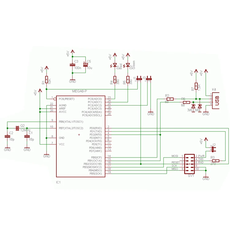
PCB design assembly smartphone pcb design

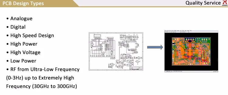

JINSEO PCB Design has the ability to complete your schematic capture and PCB layout in several different software packages including: • Cadence OrCAD/Allegro • Altium PCAD • Altium Designer |


• Acquire all information needed, reviewing and verifying the accuracy. • Schematic capture and net list generation (if not done yet). • Create part library for the project. • PCB component placement. • Submit intermediate placement to engineer for reviewing. This is usually a discussion- modification process until get approval on final placement. • PCB routing. PCB designer and engineer must maintain adequate and frequent communication during the routing process. • Complete PCB layout, finalize all documents.
|

• Bill Of Materials (BOM). • Final Net list. • Hardcopy (or electronic version) of Schematics. • Data sheets for special parts, if any. • Any special instructions on layer stack-up (i.e. Signal, Ground & Power Planes) and plane splitting. • Any drawing/detailed scratch showing board shape, size, and mounting mechanism, or heat sink, etc. • Silkscreen text identification, including Part Numbers and Revisions. • Any signals requiring special routing. • Any placement requirements or restrictions (Placement ideas is greatly helpful). |

• PCB Design Files. • Standard PCB fabrication files (Gerber & NC-Drill in standard formats). • Schematics and BOM if the schematic capture process involved in the design order. • Assembly drawings. • Assembly machine pick-place data file. • Solder paste stencil files. • Other optional files as client required. |

• Provide as accurate information of circuit design and system requirement as possible. • Avoid/minimize change on schematic after PCB layout process begins. • Reducing density and making practical requirement. • Choose responsible and highly skilled PCB designers. |
• Schematics and BOM if the schematic capture process involved in the design order.
• Assembly drawings.
• Assembly machine pick-place data file.
• Solder paste stencil files.
• Other optional files as client required.
• Provide as accurate information of circuit design and system requirement as possible. • Avoid/minimize change on schematic after PCB layout process begins. • Reducing density and making practical requirement. • Choose responsible and highly skilled PCB designers. |
We Recommend


New Arrivals
New products from manufacturers at wholesale prices


