
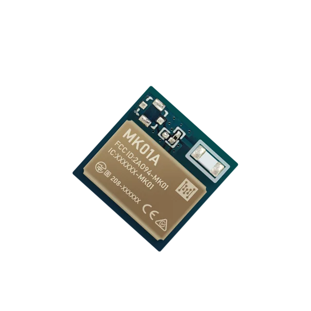
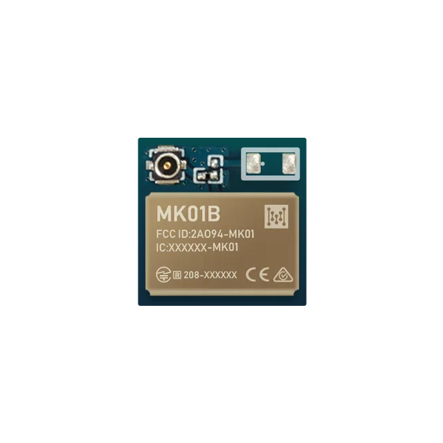
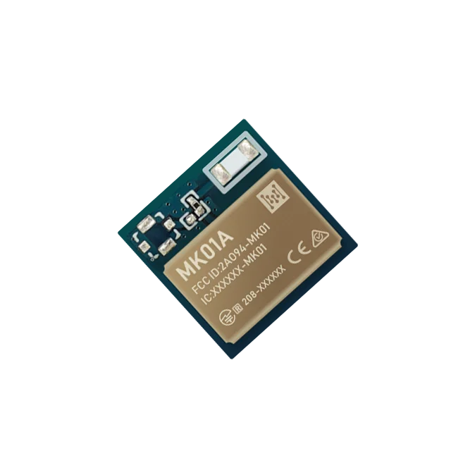
Small Bluetooth Module MK01 Full set of digital interfaces nRF52832
- Category: >>>
- Supplier: Shenzhen Moko Technology Ltd.
Share on (1600530209857):
Product Overview
Description
Small Bluetooth Module MK01 Full set of digital interfaces nRF52832
MK01 series is a powerful, highly flexible, ultra low power Bluetooth® 5 module based on Nordic® Semiconductor nRF52832 SoC solution, which has a 32 bit Arm® Cortex™-M4 CPU with floating point unit running at 64 MHz.
Product Description

MK01 module is multiprotocol capable with full protocol concurrency. It supports BLE® (Bluetooth Low Energy), including the high-speed 2 Mbps feature. Bluetooth mesh can be run concurrently with Bluetooth LE, enabling smartphones to provision, commission, configure and control mesh nodes. NFC, ANT and 2.4 GHz proprietary protocols are also supported.
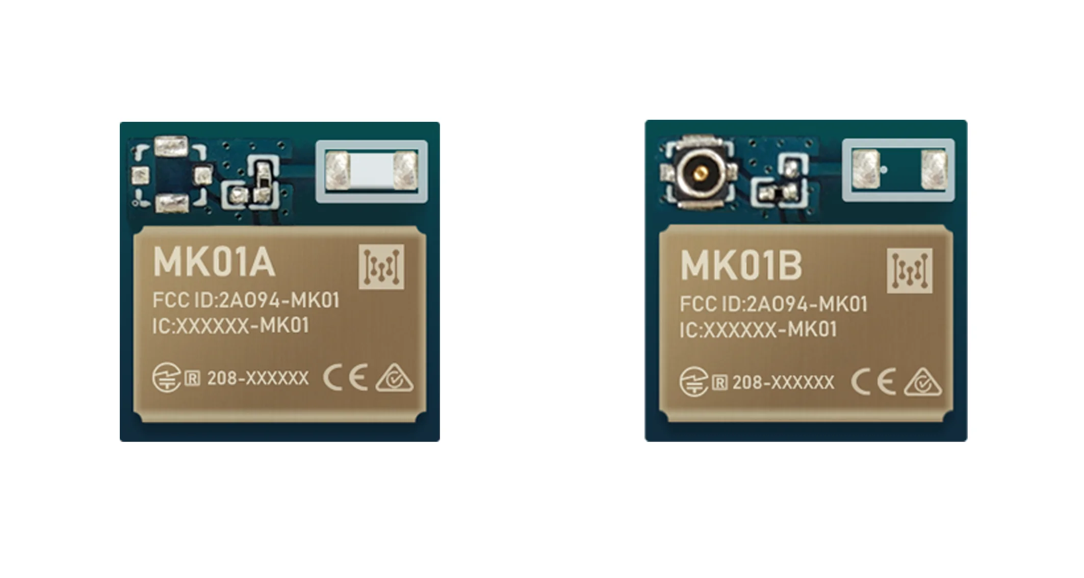
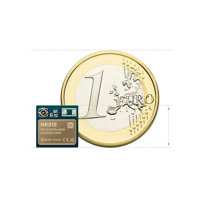
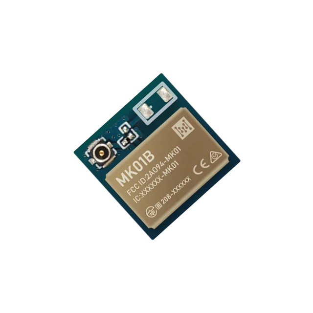
MK01 has a ultra-small size of 10mm x 10mm with 36 LGA (Land Grid Array) 0.4mm x 0.4mm pads providing 22 GPIOs of
nRF52832CIAA(WLCSP package).
nRF52832CIAA(WLCSP package).

MK01 Series BLE module features | ||||||||
Dimension | 10.0x10.0x2.0mm(with shield) | |||||||
Flash/RAM | 512KB/64KB | |||||||
Interface | UART/SPI/TWI/PDM/I2S/QDEC/PWM/ADC/NFC | |||||||
Power Supply | 1.7-3.6 V | |||||||
Operating temp | -40 to +85°C | |||||||
BLE5.0/5.1 Specification | 2 Mbps/CSA #2/Advertising Extensions | |||||||
Cover | Metal shielding with marking | |||||||
BLE Standard | BLE 4.2/5.0 | |||||||
GPIOs | 22 | |||||||
Antenna Type | Ceramic chip/u.FL Connector | |||||||
Pad package | Land Grid Array (LGA) | |||||||
Other Feature | Bluetooth mesh, ANT+, 2.4GHz | |||||||
Module Size

Pin Description

Pin No. | Name | Type | Description | nRF52 port |
1 | P0.19 | Digital I/O | General purpose I/O | P0.19 |
2 | P0.20 | Digital I/O | General purpose I/O | P0.20 |
TRACECLK | Trace port clock output | |||
3 | P0.18 | Digital I/O | General purpose I/O | P0.18 |
4 | P0.10 | Digital I/O | General purpose I/O | P0.10 |
NFC2 | NFC input | NFC antenna connection | ||
5 | P0.09 | Digital I/O | General purpose I/O | P0.09 |
NFC1 | NFC input | NFC antenna connection | ||
6 | P0.08 | Digital I/O | General purpose I/O | P0.08 |
7 | P0.06 | Digital I/O | General purpose I/O | P0.06 |
8 | P0.05 | Digital I/O | General purpose I/O | P0.05 |
AIN3 | Analog input | SAADC/COMP/LPCOMP input | ||
9 | P0.00 | Digital I/O | General purpose I/O | P0.00 |
XL1 | Analog input | Connection for 32.768 kHz crystal (LFXO) | ||
10 | P0.01 | Digital I/O | General purpose I/O | P0.01 |
XL2 | Analog input | Connection for 32.768 kHz crystal (LFXO) | ||
11 | DEC4 | Power | 1.3 V regulator supply decoupling Input from DC/DC converter. Output from 1.3 V LDO | DEC4 |
12 | GND | Power | Electrical Ground | VSS |
13 | VCC | Power | Power supply. An internal 4.7 µF bulk capacitor is included on the module. However, it is good design practice to add additional bulk capacitance as required for your application, i.e. those with heavy GPIO usage and/or current draw. | VDD |
14 | DCC | Power | DC/DC converter output | DCC |
15 | P0.02 | Digital I/O | General purpose I/O | P0.02 |
AIN0 | Analog input | SAADC/COMP/LPCOMP input | ||
16 | P0.30 | Digital I/O | General purpose I/O 8 | P0.30 |
AIN6 | Analog input | SAADC/COMP/LPCOMP input | ||
17 | P0.03 | Digital I/O | General purpose I/O | P0.03 |
AIN1 | Analog input | SAADC/COMP/LPCOMP input | ||
18 | P0.04 | Digital I/O | General purpose I/O | P0.04 |
AIN2 | Analog input | SAADC/COMP/LPCOMP input | ||
19 | P0.25 | Digital I/O | General purpose I/O | P0.25 |
20 | GND | Power | Electrical Ground | VSS |
21 | GND | Power | Electrical Ground | VSS |
22 | P0.21 | Digital I/O | General purpose I/O | P0.21 |
RESET | Configurable as pin reset | |||
23 | P0.14 | Digital I/O | General purpose I/O | P0.14 |
TRACEDATA[3] | Trace port output | |||
24 | P0.15 | Digital I/O | General purpose I/O | P0.15 |
TRACEDATA[2] | Trace port output | |||
25 | P0.16 | Digital I/O | General purpose I/O | P0.16 |
TRACEDATA[1] | Trace port output | |||
26 | SWDCLK | Digital input | Serial wire debug clock input for debug and programming | SWDCLK |
27 | SWDIO | Digital I/O | Serial wire debug I/O for debug and programming | SWDIO |
28 | P0.28 | Digital I/O | General purpose I/O | P0.28 |
AIN4 | Analog input | SAADC/COMP/LPCOMP input | ||
29 | P0.29 | Digital I/O | General purpose I/O | P0.29 |
AIN5 | Analog input | SAADC/COMP/LPCOMP input | ||
30 | P0.26 | Digital I/O | General purpose I/O | P0.26 |
31-36 | GND | Power | Electrical Ground | VSS |
Block Diagram

Evaluation Board
MK01-KIT evaluation board is applicable for MK01A and MK01B Bluetooth® module. This board provides you with a quick and easy way to develop MK01 series module or even Nordic® nRF52832 solution.
It is a full featured evaluation board that provides a complete I/O pin and debug pin(SWD) out to headers, external 32.768 kHz crystal setup, DC/DC regulator setup, power port over USB Type-C, NFC antenna FPC connector, one RESET button, one user button and one user RGB-LED. The evaluation boards also provide the option to be powered from a CR2032 coin cell battery and have current sense hole to allow for convenient current measurements.


Application and Solution

Packing & Delivery
Samples:
we would send samples via DHL Express within about 2 days after payment, then you would receive them in about 4 to 5 days.
Orders:
bulk orders usually take about 2 to 3 weeks after payment received
we would send samples via DHL Express within about 2 days after payment, then you would receive them in about 4 to 5 days.
Orders:
bulk orders usually take about 2 to 3 weeks after payment received

Company Profile


Our Customers&Buyers Feedback

We Recommend


New Arrivals
New products from manufacturers at wholesale prices


