PE Embossed Wafer Separators Wafer Pads 11 inch interleaf for wafer
- Category: Plastic Film >>>
- Supplier: Shanghai Haouger Electronic Technology Co. Ltd.
Share on (1600537267023):
Product Overview
Description
Product Display

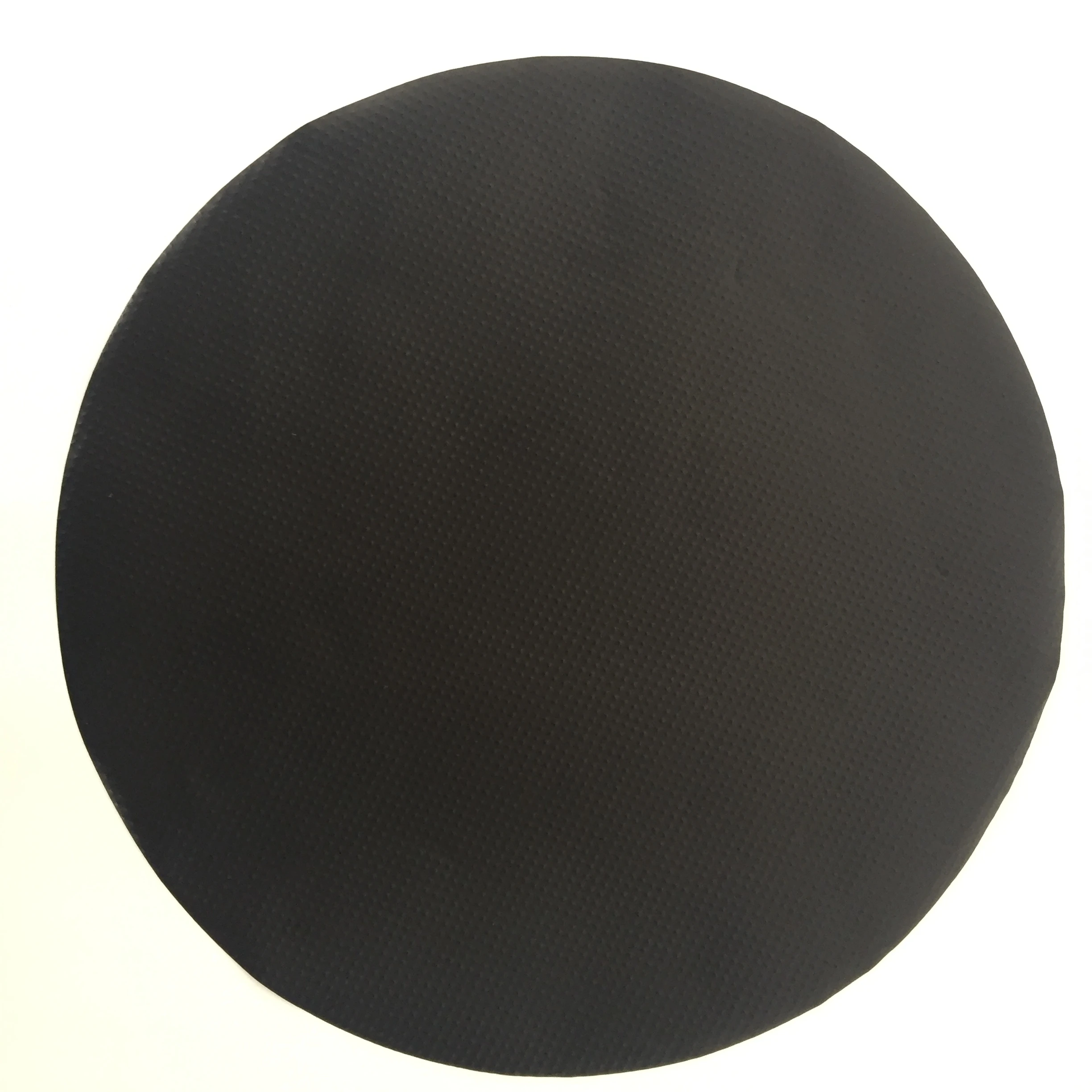
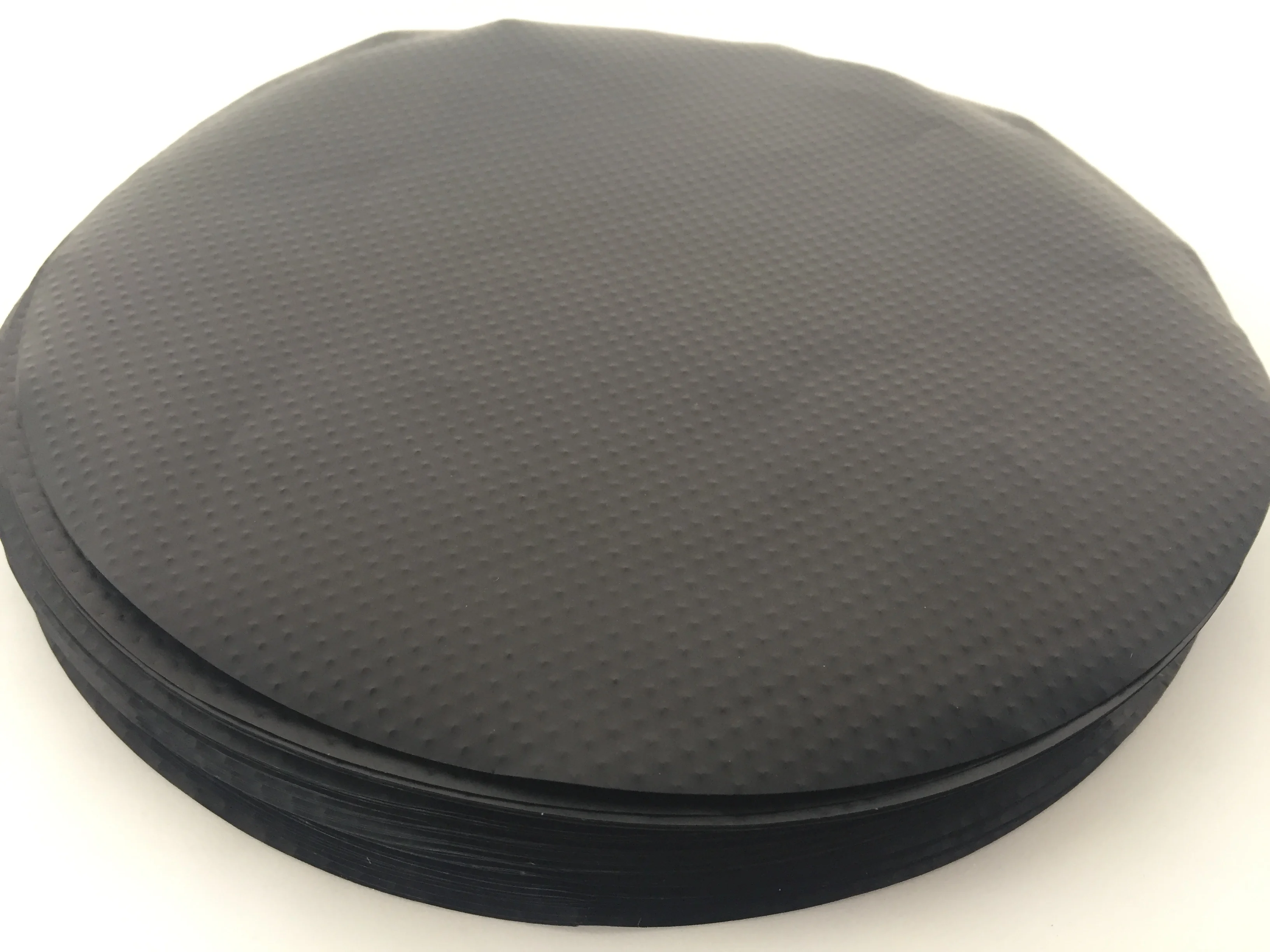
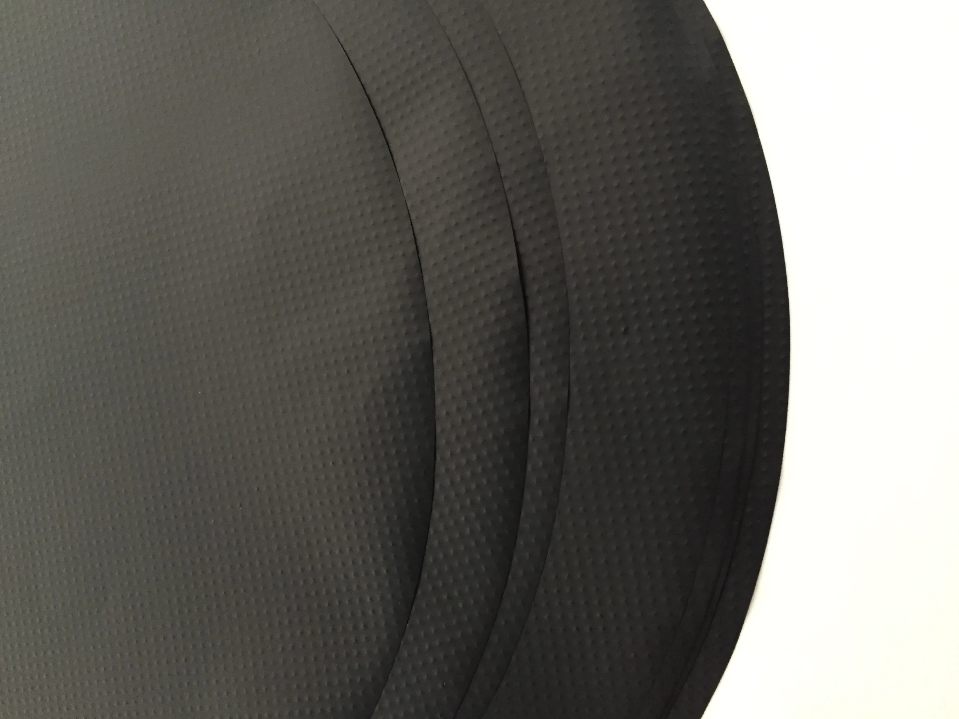
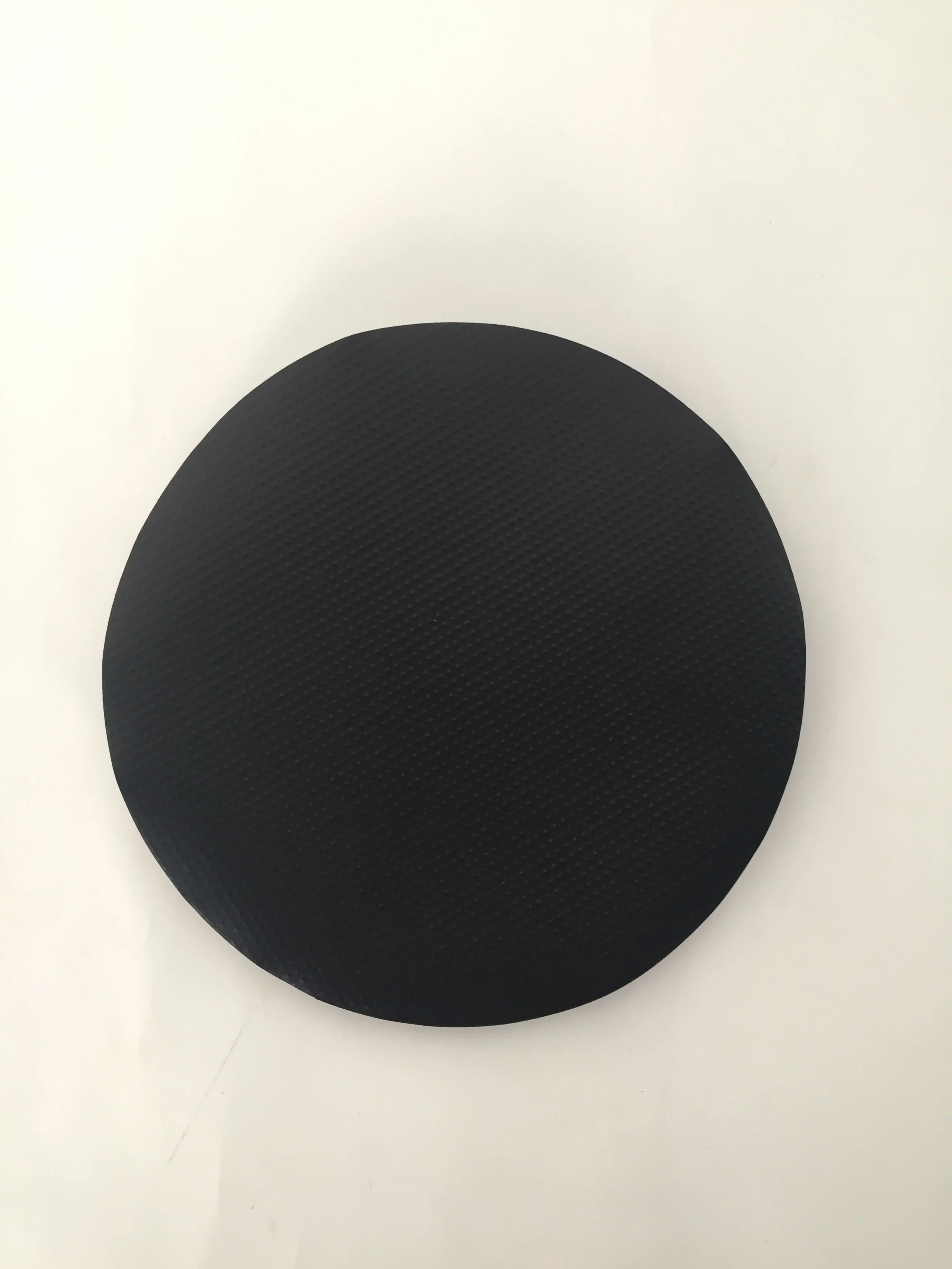
The WAFER PAD
A waf pad is also called an anti-static accumulation pap, a silicon wafer paper, a buffer pad in a semiconductor waf box, A solar wafer buffer pad, a semiconductor wafer box inner pad, a PCB buffer pad, a conductive spacer, a black wafer spacer, an anti-static wafer spacer, a conductive wafer spacer, a circular wafer spacer, a wafer square, and the surface treatment process thereof is also called an anti-static black embossed wafer pad, an embossed wafer square, and the like.
This product is made of permanent conductive or anti-static film through hot-pressing, die-cutting. Film surface can be made smooth, can also be made according to the requirements of a variety of patterns. The product can be made into any size and shape according to the requirements, and the finished product has excellent dimensional stability, clean appearance, no powder falling and no dust. Protruding patterned wafer pads can not only effectively prevent the product from electrostatic damage, but also play a certain role in cushioning.
Detail image


Related Products
Company Information
Founded in 2005, Shanghai HAOUGER Electronic Technology Co., Ltd. is one of the earliest domestic companies specializing in the research and development of carbon black, graphene films and products. There are two Joint venture factory of shareholders in Hebei Province (located in Gucheng County Economic and Technological Development Zone, Hengshui City, Hebei Province, with a workshop area of 6,600 square meters) and Jiangsu Province (located in Xiangshui County Economic Development Zone, Yancheng City, Jiangsu Province, with a workshop area of 5,000 square meters).
Both Joint venture factory of shareholders and testing equipments are available in the factory and the main production processes have been automated operations. Our main raw materials for Joint venture factories are independently developed and prepared by the graphene industry consortium. The carbon black and graphene thin film products have complete functions and stable properties, which can meet various functions and customization requirements. In addition, through strict control of the production process, the carbon black film products have successfully replaced the imported products in many high-precision fields. After more than 20 years of accumulation and precipitation, the scale of professional production makes our conductive coil film-related products more cost-effective. Currently, our products have already been recognized by the majority of users in various industries , and exported all over the world in batches through a variety of channels.
Since the establishment of the company, we have been adhering to the professional, dedicated, diligent and patient business purposes, accomplishing every sing mission expected by our customers. With the growth of the company, we are determined to build the company into a first-class "service-oriented company" through sincere cooperation with customers at home and abroad, through the continuous strengthening of our own management and the joint efforts of all employees, to create more value for the majority of customers!


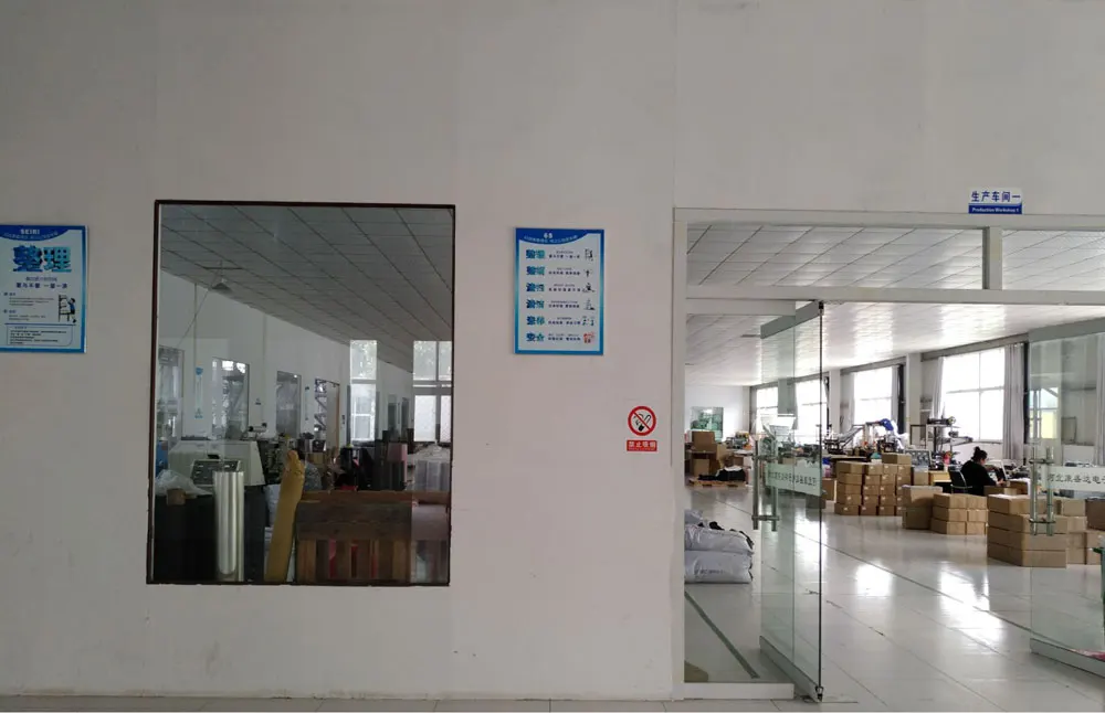
Workshop Pictures


Our Advantages

Packing & Delivery
To better ensure the safety of your goods, professional, environmentally friendly, convenient and efficient packaging services will be provided.


FAQ
Q1:Whether to support customization?
Yes.
Q2:Whether to support sample service?
1.Free sample for 1 square meter.Buyer pay the express fee .
2.Support for customized services,from 5000 square meters
Yes.
Q2:Whether to support sample service?
1.Free sample for 1 square meter.Buyer pay the express fee .
2.Support for customized services,from 5000 square meters
We Recommend


New Arrivals
New products from manufacturers at wholesale prices


