
Semiconductor Material 6H SiC Wafer Single Crystal (Silicon Carbide)
- Category: Semiconductors >>>
- Supplier: Shanghai Xinkehui New Material Co. Ltd.
Share on (1600546812825):
Product Overview
Description
Product Description

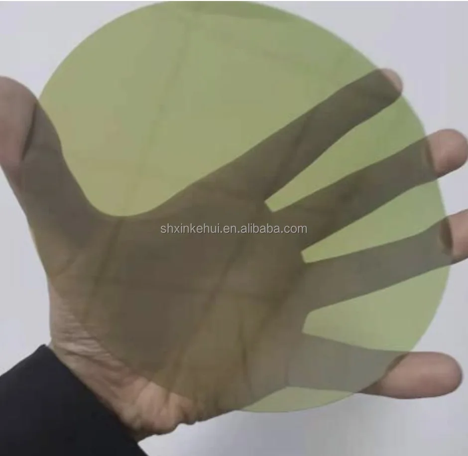
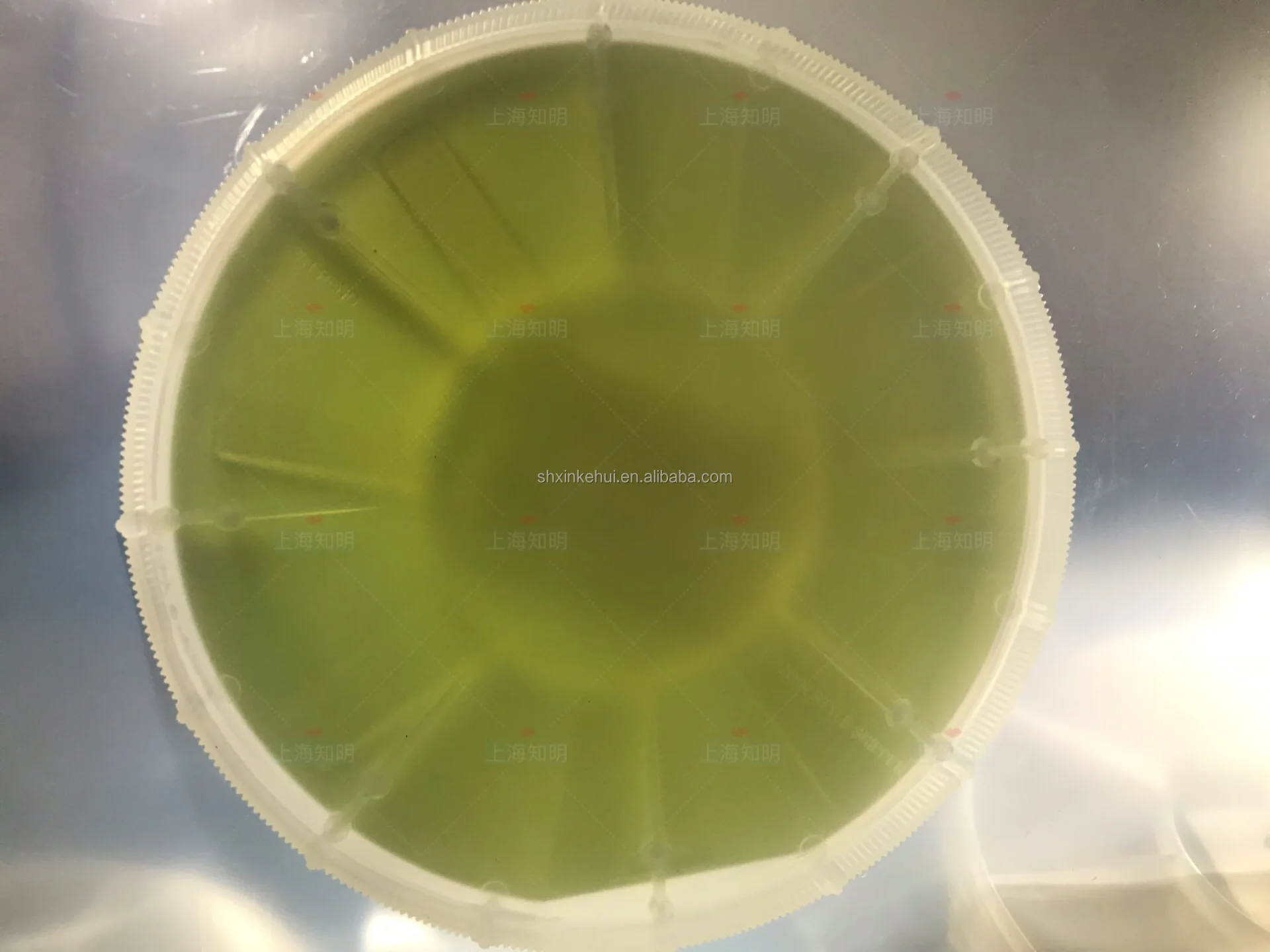
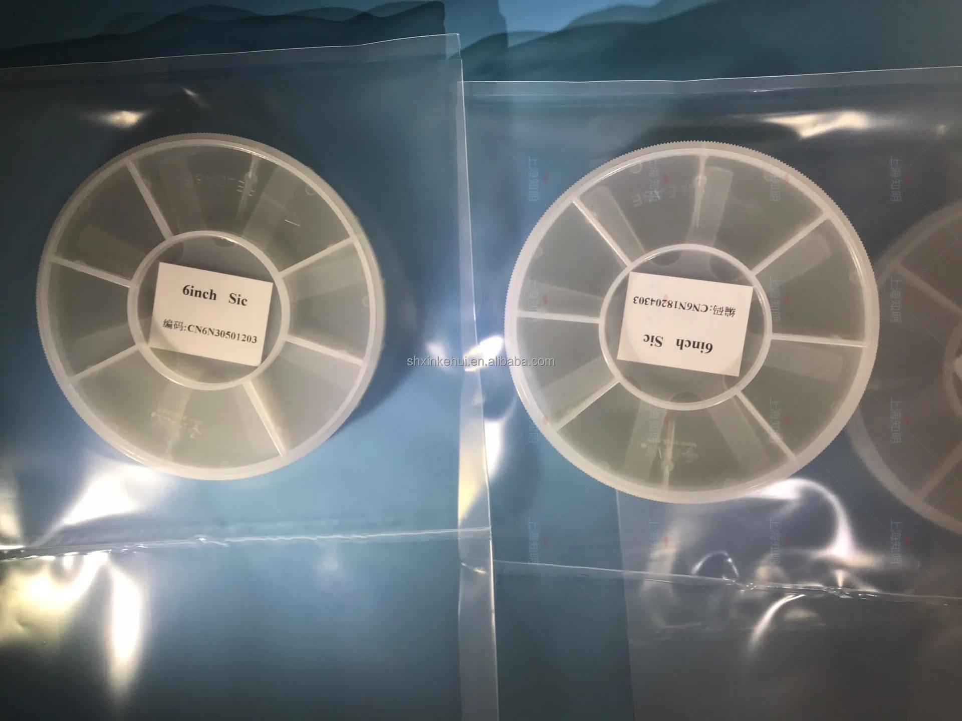
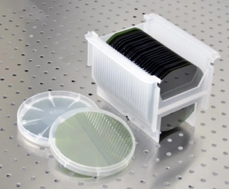
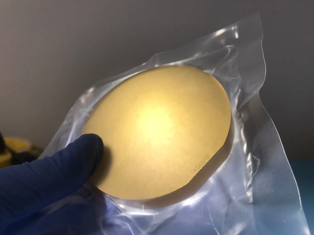
SiC(Silicon Carbide) Wafer
Silicon carbide (SiC), also known as carborundum, is a semiconductor containing silicon and carbon with chemical formula SiC. SiC is used in semiconductor electronics devices that operate at high temperatures or high voltages, or both.SiC is also one of the
important LED components, it is a popular substrate for growing GaN devices, and it also serves as a heat spreader in high-power
LEDs.
important LED components, it is a popular substrate for growing GaN devices, and it also serves as a heat spreader in high-power
LEDs.
------------------------------------------
Shanghai XInkehui New Material Also can supply high customized sic wafer to our customers
Customzied size/2inch/3inch/4inch/6inch 6H-N/4H-SEMI/ 4H-N SIC ingots/High purity 4H-N 4inch 6inch dia 150mm silicon carbide
single crystal (sic) substrates wafers
single crystal (sic) substrates wafers

SiC Wafer Application
* 1 high frequency and high power electronic devices Schottky diodes, JFET, BJT, PiN, diodes, IGBT, MOSFET
* 2 to electronic devices: mainly used in GaN/SiC blue LED substrate material (GaN/SiC) LED
* 2 to electronic devices: mainly used in GaN/SiC blue LED substrate material (GaN/SiC) LED
Common Size
4H-N Type / High Purity SiC wafer/ingots 2 inch 4H N-Type SiC wafer/ingots 3 inch 4H N-Type SiC wafer 4 inch 4H N-Type SiC wafer/ingots 6 inch 4H N-Type SiC wafer/ingots | 4H Semi-insulating / High Purity SiC wafer 2 inch 4H Semi-insulating SiC wafer 3 inch 4H Semi-insulating SiC wafer 4 inch 4H Semi-insulating SiC wafer 6 inch 4H Semi-insulating SiC wafer |
6H N-Type SiC wafer 2 inch 6H N-Type SiC wafer/ingot | Customzied size for 2-6inch |

Specification
Property | 4H-SiC, Single Crystal | 6H-SiC, Single Crystal |
Lattice Parameters | a=3.076 Å c=10.053 Å | a=3.073 Å c=15.117 Å |
Stacking Sequence | ABCB | ABCACB |
Mohs Hardness | ≈9.2 | ≈9.2 |
Density | 3.21 g/cm3 | 3.21 g/cm3 |
Therm. Expansion Coefficient | 4-5×10⁻⁶/K | 4-5×10⁻⁶/K |
Refraction Index @750nm | no = 2.61 ne = 2.66 | no = 2.60 ne = 2.65 |
Dielectric Constant | c~9.66 | c~9.66 |
Thermal Conductivity (N-type, 0.02 ohm.cm) | a~4.2 W/cm·K@298K c~3.7 W/cm·K@298K | |
Thermal Conductivity (Semi-insulating) | a~4.9 W/cm·K@298K c~3.9 W/cm·K@298K | a~4.6 W/cm·K@298K c~3.2 W/cm·K@298K |
Band-gap | 3.23 eV | 3.02 eV |
Break-Down Electrical Field | 3-5×10⁶V/cm | 3-5×10⁶V/cm |
Saturation Drift Velocity | 2.0×10⁵m/s | 2.0×10⁵m/s |
4H-N 4 inch diameter Silicon Carbide (SiC) Substrate Specification
2 inch diameter Silicon Carbide (SiC) Substrate Specification
Grade | Zero MPD Grade | Production Grade | Research Grade | Dummy Grade | |||
Diameter | 100. mm±0.2 mm or other customized size | ||||||
Thickness | 1000±25 um Or other customized thickness | ||||||
Wafer Orientation | Off axis : 4.0° toward <1120> ±0.5° for 4H-N/4H-SI On axis : <0001>±0.5° for 6H-N/6H-SI/4H-N/4H-SI | ||||||
Micropipe Density | ≤0 cm-2 | ≤2 cm-2 | ≤5 cm-2 | ≤30 cm-2 | |||
Resistivity 4H-N | 0.015~0.028 Ω•cm | ||||||
Resistivity 4/6H-SI | ≥1E7 Ω·cm | ||||||
Primary Flat | {10-10}±5.0° or round shape | ||||||
Primary Flat Length | 18.5 mm±2.0 mm or round shape | ||||||
Secondary Flat Length | 10.0mm±2.0 mm | ||||||
Secondary Flat Orientation | Silicon face up: 90° CW. from Prime flat ±5.0° | ||||||
Edge exclusion | 1 mm | ||||||
TTV/Bow /Warp | ≤10μm /≤10μm /≤15μm | ||||||
Roughness | Polish Ra≤1 nm / CMP Ra≤0.5 nm | ||||||
Cracks by high intensity light | None | 1 allowed, ≤2 mm | Cumulative length ≤ 10mm, single length≤2mm | ||||
Hex Plates by high intensity light | Cumulative area ≤1% | Cumulative area ≤1% | Cumulative area ≤3% | ||||
Polytype Areas by high intensity light | None | Cumulative area ≤2% | Cumulative area ≤5% | ||||
Scratches by high intensity light | 3 scratches to 1×wafer diameter cumulative length | 5 scratches to 1×wafer diameter cumulative length | 5 scratches to 1×wafer diameter cumulative length | ||||
edge chip | None | 3 allowed, ≤0.5 mm each | 5 allowed, ≤1 mm each | ||||
SiC Wafer Display


-------------------------------------------------------------------------------------------------------------
Related Products
Shanghai Xinkuhui New Material Co. Ltd. professional in the area of all kind of semiconductor crystal
(GaN; SiC; Sapphire; GaAs; InP; Silicon; MgO, LT/LN; etc.)
if you are interested, your are welcome to visit our channel
(GaN; SiC; Sapphire; GaAs; InP; Silicon; MgO, LT/LN; etc.)
if you are interested, your are welcome to visit our channel
Packing & Delivery


Company Profile

Shanghai Xinkehui New Material Co. Ltd.,
Main Market:
North America, South America, Western Europe, Eastern Europe, Middle East, Africa, WorldwideBusiness Type:
Manufacturer, Agent, Importer, Exporter, Trading Company
Annual Sales:
1000000-1500000
Export p.c:
80% - 90%
Manufacturer, Agent, Importer, Exporter, Trading Company
Annual Sales:
1000000-1500000
Export p.c:
80% - 90%
Shanghai Xinkehui Company. locates in the city of Shanghai, Which is the best city of China, and our factory is founded in
Wuxi city in 2014.
We specialize in processing a variety of materials into wafers, substrates and customized optical glass parts.components widely used in electronics, optics, optoelectronics and many other fields. We also have been working closely with many domestic and oversea universities, research institutions and companies, provide customized products and services for their R&D projects. It's our vision to maintaining a good relationship of cooperation with our all customers by our good reputations.


Office building Office Workshop Our Logo
FAQ
Q: What's the way of shipping and cost?
(1) We accept DHL, Fedex, TNT, UPS, EMS, SF and etc.
(2) If you have your own express account, it's great.
Q: How to pay?
(1) T/T, PayPal, West Union, MoneyGram and
Assurance payment on Alibaba and etc..
(2) Bank Fee: West Union≤USD1000.00),
T/T -: over 1000usd ,please by t/t
Q: What's the deliver time?
(1) For inventory: the delivery time is 5 workdays.
(2) For customized products: the delivery time is 7 to 25 workdays. According to the quantity.
Q: Can I customize the products based on my need?
Yes, we can customize the material, specifications and optical coating for your optical components based on your needs.
↓↓↓If you are interested in our SiC Wafer or other semiconductor wafer, please leave us your inquiry↓↓↓
We Recommend


New Arrivals
New products from manufacturers at wholesale prices