
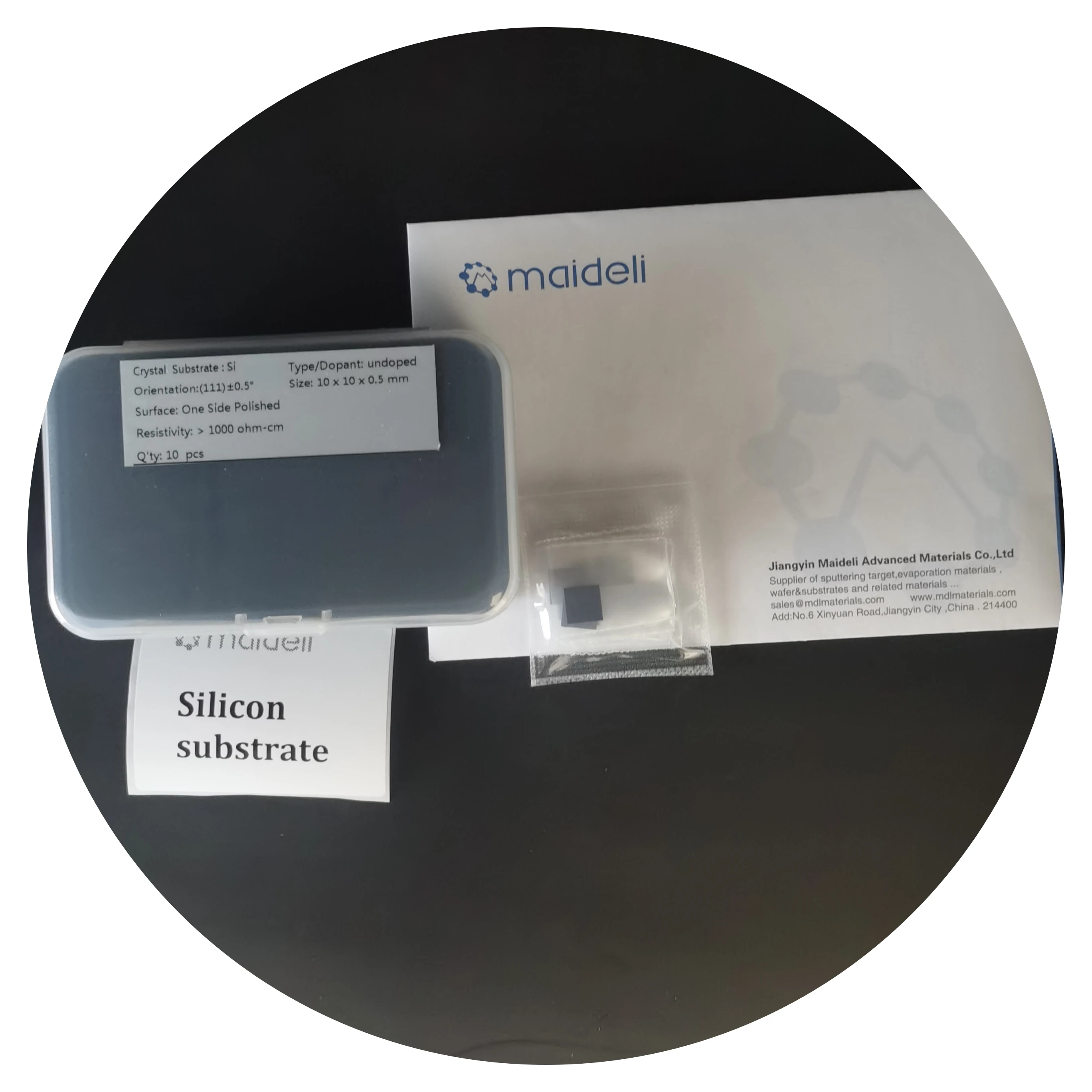
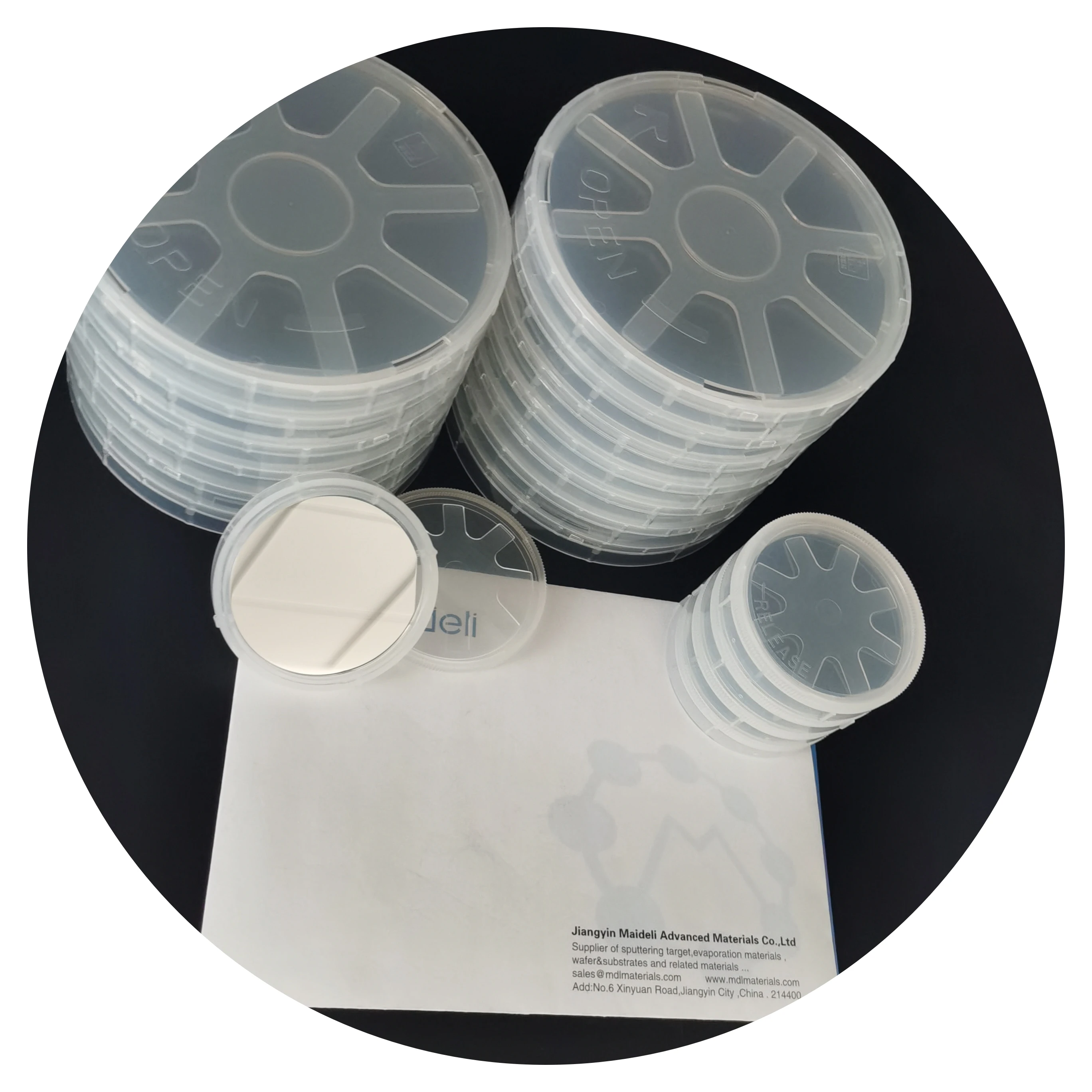
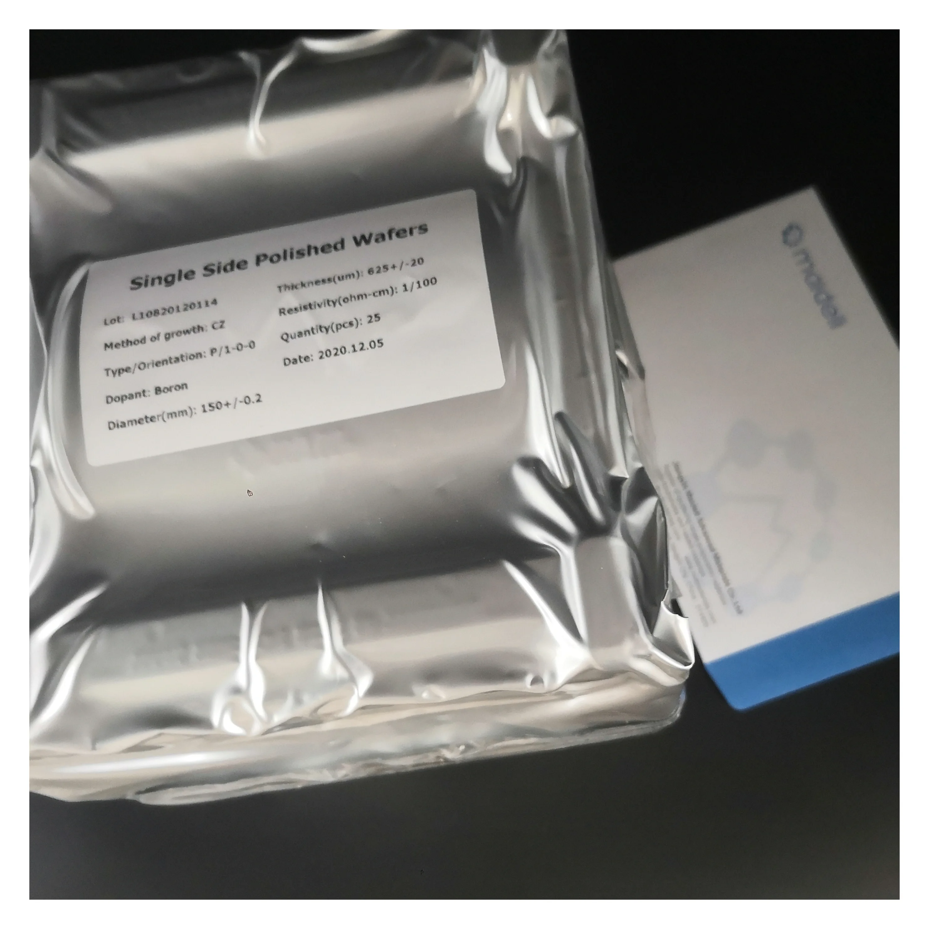
Intrinsic Silicon wafer Si wafer resistivity >10.000 ohm cm orientation 100 , SSP ,with size 1inch diameter
- Category: >>>
- Supplier: Jiangyin Maideli Advanced Materials Co. Ltd
Share on (1600550402418):
Product Overview
Description
Product Description
Specification
Monocrystalline silicon is excellent cost –effective integrated infrared optical materials ,used to make infrared optical lenses
,is mainly used in the thermal imaging system ,flir ,high-tech areas like mobile sensors . Number or the fine laser reflector
material, compared with other mirror materials such as copper and molybdenum , number because of it’s good thermal conductivity
,excellent thermal stability ,low thermal expansion cofficient and relatively low
density ,low cost ,easy to the advantages of the precision machining ,is currently the CO2 laser reflector preferred base material
. Optical number according to the crystal growth mode can be divided into the czochralski(CZ) silicon single crystal and zone
melting (FZ) single crystal silicon .
item | value |
Place of Origin | China |
Jiangsu | |
Brand Name | Maideli |
Model Number | Si-wafer |
Type | Silicon Wafer |
Product name | Silicon Wafer |
Material | Silicon |
Diameter | 3 inch |
Thickness | 100~1000um |
Type | N Type / P Type |
Orientation | 111 |
Resistivity | 0.002~25000 Ω.cm |
Flatness TIR | <3um |
Warping degree TTV | <10um |
flexibility BOW | <10um |
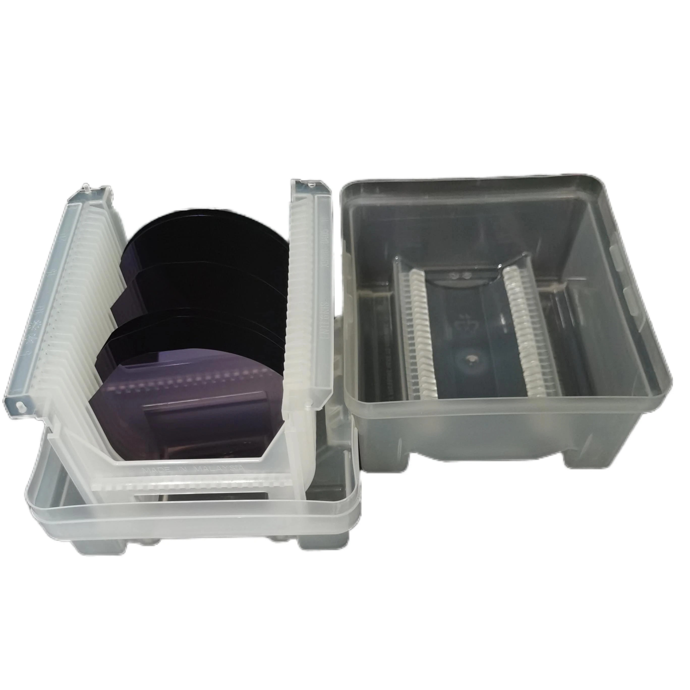
Packing & Delivery
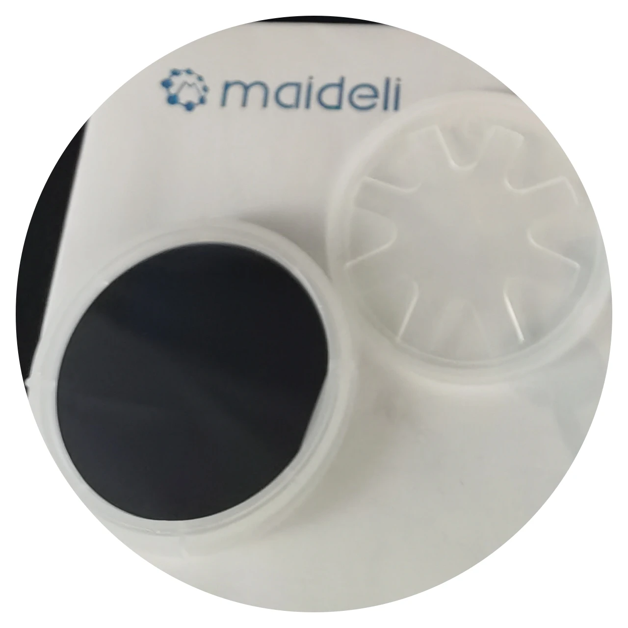
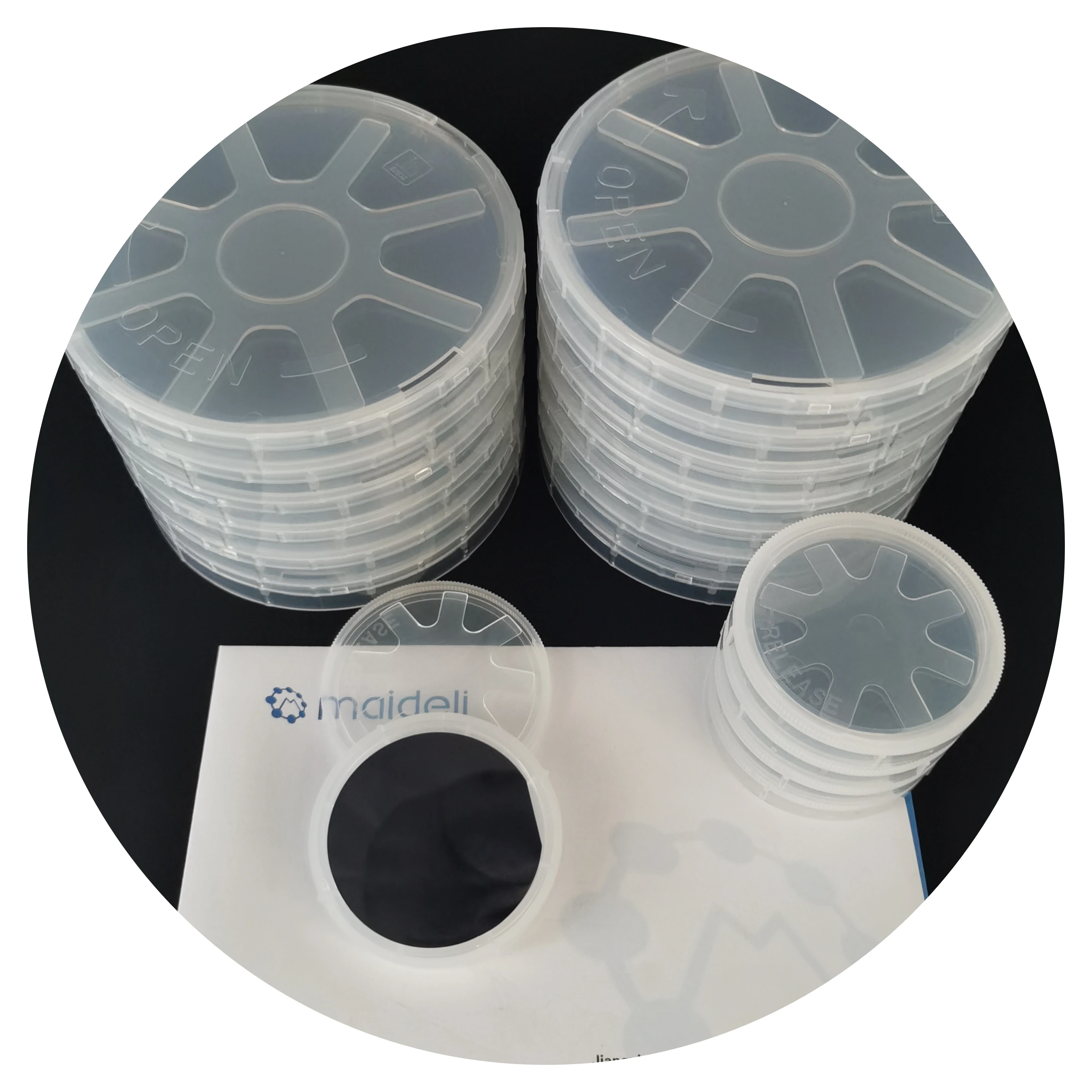
Packing Details : vacuumed polybag each pc
Delivery Details : 3-30 days after order
1. Sampling packing
2.Order packing--Packed in 100 grade plastic bag under 1000 class clean room
3. Carton packing with good protection
Shipping

Transportation way
We can arrange the shipment via FedEx,DHL,TNT,UPS,SF ,etc...

Transportation Time
1)Sampling Shipping : 3 to 7 days ,according to local customs .
2)Commercial shipping : 4 to 10 days ,according to customs .
Related Products
Monocrystal Substrate
New Crystal | ||||||||
DyScO3 | GdScO3 | PrScO3 | NdScO3 | SnO2 | ||||
MnO | CeO2 | Cu2O | Fe3O4 | Fe2O3 | ||||
ZnO/Al2O3 | ||||||||
superconducting thin film | ||||||||
SrTiO3 | LaAlO3 | YSZ | MgO | NdGaO3 | ||||
KTaO3 | SrLaAlO4 | |||||||
Functional epitaxial thin films | ||||||||
SiO2 + Si | GaN on Sapphire wafer | Pt/Ti/SiO2/Si wafer | ||||||
magnet ferroelectric thin film substrate | ||||||||
GGG substrate | Nb:SrTiO3 substrate | Fe:SrTiO3 substrate | PMN-PT substrate | |||||
Photo Transistor substrate | ||||||||
TiO2 Rutile substrate | SiO2 quartz monocrystal substrate | quartz glass substrate | YAlO3 substrate | YAG substrate | ||||
LiNbO3 substrate | LiTaO3 substrate | |||||||
semiconducting crystal substrate | ||||||||
SOI Si+SiO2+Si | Ge substrate | Si substrate | InP substrate | InAs substrate | ||||
InSb substrate | ||||||||
fluo-chloride crystal substrate | ||||||||
MgF2 substrate | CaF2 substrate | BaF2 substrate | LiF substrate | KCl substrate | ||||
NaCl substrate | KBr substrate | |||||||
III-V crystal substrate | ||||||||
Sapphire wafer | GaN monocrystal substrate | LiAlO2 substrate | MgAl2O4 substrate | |||||
II-VI crystal substrate | ||||||||
ZnO high resistivity substrate | ZnO low resistivity substrate | Ga:ZnO substrate | SiC substrate | |||||
ceramic substrate | ||||||||
Al2O3 96% substrate | AlN ceramic substrate | YSZ ceramicsubstrate | ||||||
Other materials | ||||||||
Cu metal monocrystalsubstrate | Al metal monocrystalsubstrate | Mg metal monocrystalsubstrate | KTa(1-x)Nb(x)O3 | K9 glass substrate | ||||
Sapphire Tube | Ruby Tube | |||||||
Company Introduction

About Us
Maideli Advanced Materials is a high-tech enterprise who professionally engaged in R&D ,production ,Sales and service of
Sputtering Target ,Evaporation Materials ,Wafers, Quartz and Ceramic Products .
Maideli has been focus on the service of market in optic, optical communication ,panel display ,solar panel,TP,IC,LED chips
,decorative coating ,tooling coating ,low emission glass and so on . We specialize in producing high purity film coating materials with the highest possible density and smallest possible average grain sizes for use in semiconductor, chemical vapor deposition (CVD) and physical vapor deposition (PVD) display and optical applications.
As always , Maideli starts with what the customer required and with Satisfied end . The company continue to strengthen
technological innovation ,strengthen production management ,accelerate the implementation of the technology and quality of the enterprise policy ,to provide better ,more detailed ,faster service to customers
Exhibition


FAQ
Q: Are you trading company or manufacturer ?
A: We are factory.
Q: How long is your delivery time?
A: Generally it is 3~7 days if the goods are in stock. or it is 15-20 days if the goods are not in stock, it is according to quantity.
Q: Do you provide samples ? is it free or extra ?
A: Yes, we could offer the sample ,but we need to take the sample fee .
Q: What is your terms of payment ?
A: Payment<=1000USD, 100% in advance. Payment>=1000USD, 30% T/T in advance ,balance before shippment.
We Recommend

New Arrivals
New products from manufacturers at wholesale prices


