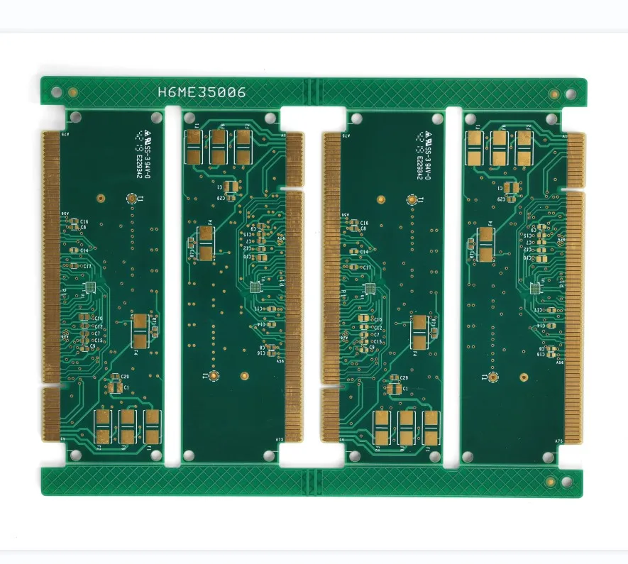
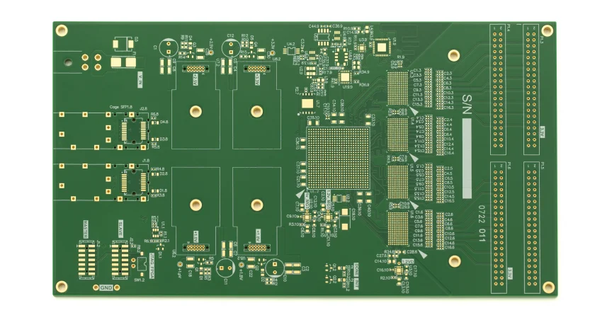
JINHUA high quality FR4 double sided custom multilayer Gold Finger pcb
- Category: >>>
- Supplier: Jinhua Technology (shenzhen) Co. Ltd.
Share on (1600580105185):
Product Overview
Description
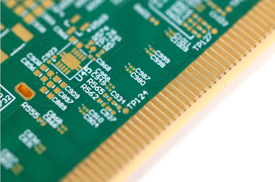
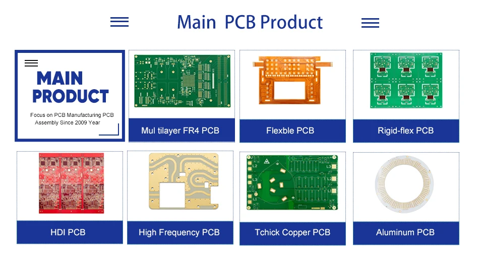
Multilayer PCB is a Printed Circuit Board with more than 2 layers. A Double-Sided PCB has two conductive layers on top and bottom of the PCB substrate. A Multilayer PCB must have a minimum of 3 conductive layers of conductive material or copper layer. All the layers are interconnected with copper plated holes. The layers can be 4, 6, 8…upto 32 layers.
Product Description
| JINHUA PCB Standard Capability | |||
| Item | Process | Manufacturing Capability | Remark |
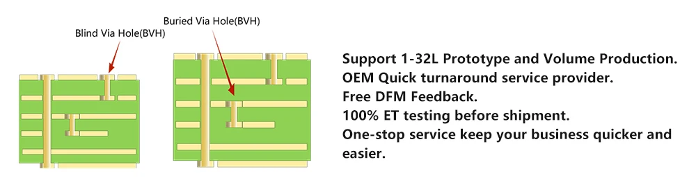
| 1 | Surface Finishing | HASL, HASL LF, ENIG, gold fingers plating, OSP, Immersion Ag, Immersion Sn, Carbon Ink, peelable mask, plug vias with resin | |
| 2 | Board Thickness | 0.1 MM ~ 8.0 MM | |
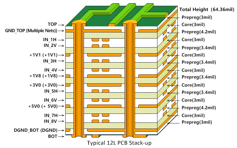
| 3 | Layers | 1 ~ 32 L | |
| 4 | Material | Brand: KB, ITEQ, Shengyi, Huazheng,NanYa, CEM, Arlon,Rogers, Teflon, Polymide, panasonic, Aluminum Base, Halogen Free,Peters Soldermask,Kapton high temperature tape, Taiyo Ink | |
| TG: low to high, TG135 to TG180; CTI: 175 to 600 | |||
| 5 | Board Size | Max board size:650 x 1200 MM; Min board size: 3*3 MM | |
| 6 | Inner Layer | (1) ring of line: single sided 4mil | Aspect ratio:10: 1 |
| (2) min trace w/s for 1 OZ:3 mil/2.6mil | Max finished copper thickness:18/18 oz | ||
| (3) hole to line or pad spacing: min 6mil | |||
| 7 | Drilling | (1) min finished hole size: laser 0.1mm mechanical 0.15mm | |
| (2) PTH hole size tolerance: ± 3 mil,NPTH hole size tolerance: ± 2 mil | hole position registration tolerance: ± 2 mil | ||
| (3) min slot size:0.55 mm | |||
| 8 | Outer Layer | (1) 1oz: 3/3 mil, 2oz:5/5 mil | Max finished copper thickness:18/18 oz |
| 9 | Plating | (1) hole wall copper thickness 1-10 mil | |
| (2) 10:1 | |||
| 10 | Soldermask | (1) min soldermaks bridge 4mil | min PAD 20 mil |
| 11 | Silkscreen | Color:white, black, yellow, red...etc. | Serial number, Barcode, QR code |
| 12 | Profiling | (1) Tolerance of outline: ± 0.1mm | |
| (2) V-CUT Angle: 30 degree & 45 degree | min V-Cut width 75 MM | ||
| (3) Depth:Board thickness≥1.2 mm Remain thicknss: 1/3; Board thickness≤1.2 mm, remain thickness 20 mil (0.5 mm) | min distance V-Cut to copper 0.4 MM | ||
| (4) Bevelling angle/depth: 20°/1.8 mm;30° /1.0 mm;45°/0.5 mm;tolerance:± 5°/± 0.2 mm | |||
| 13 | Bow and Twist | 1L≤1.0% 2L≤0.75% Multi layers≤0.75% | |
| 14 | Monthly Capcity | 120,000 M2 | |
| Layer | Quick Turn/Usual Time | Mass Production |
| 2L | 24 hours/4-5 days | 8-10 days |
| 4L | 48 hours/6-7 days | 10-12 days |
| 6L | 72 hours/7-8 days | 12-14 days |
| 8L | 72 hours/8-10 days | 16-18 days |
| 10L | 96 hours/12-14 days | 18-20 days |
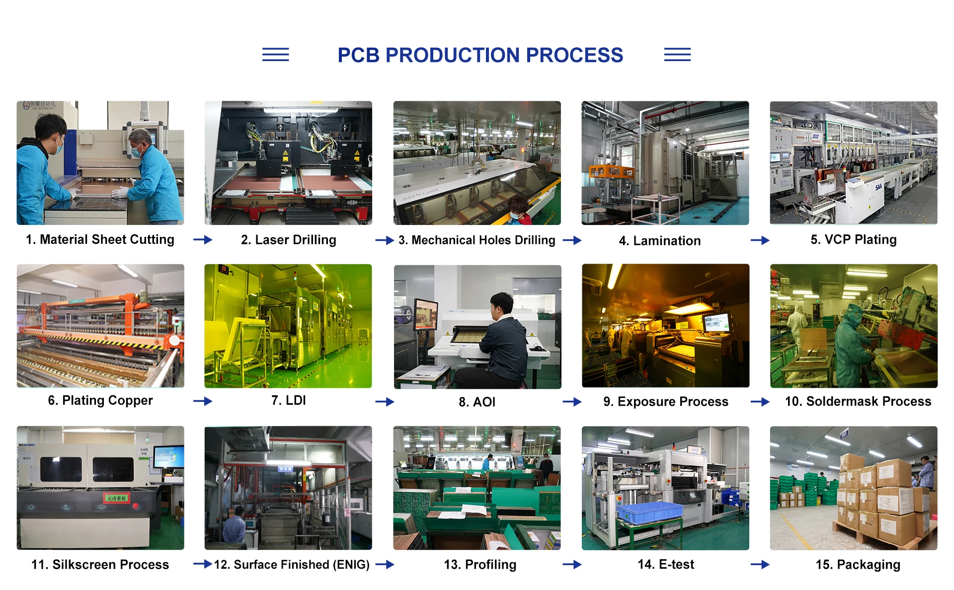
Production Process
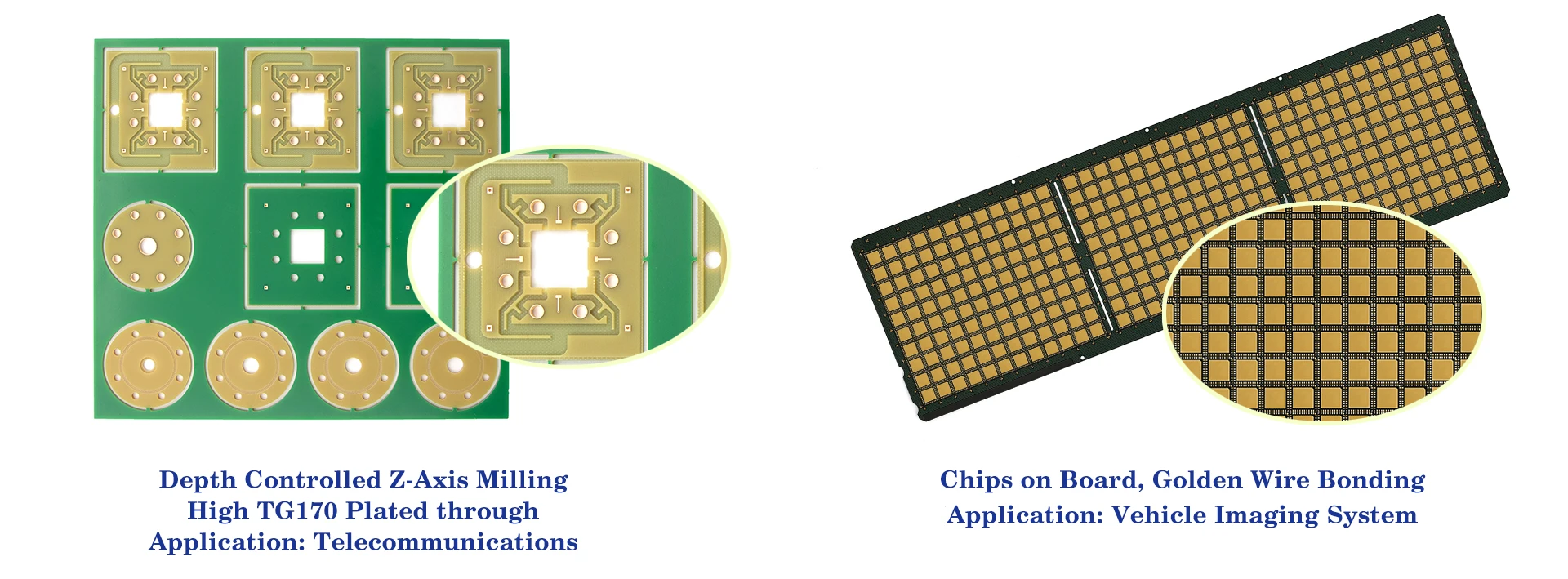
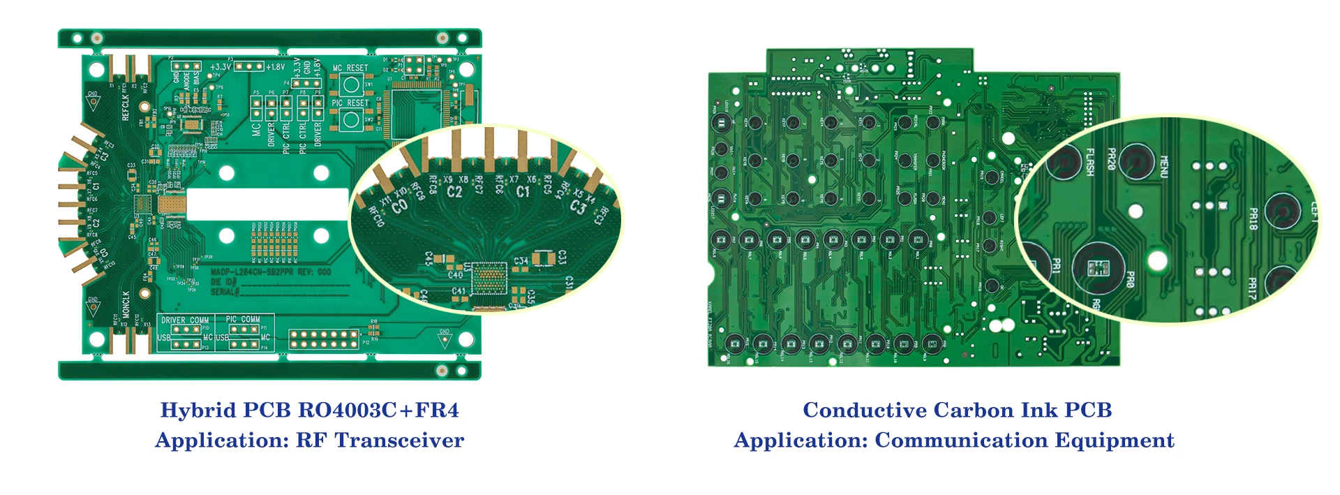
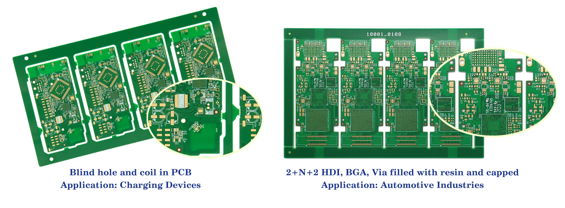
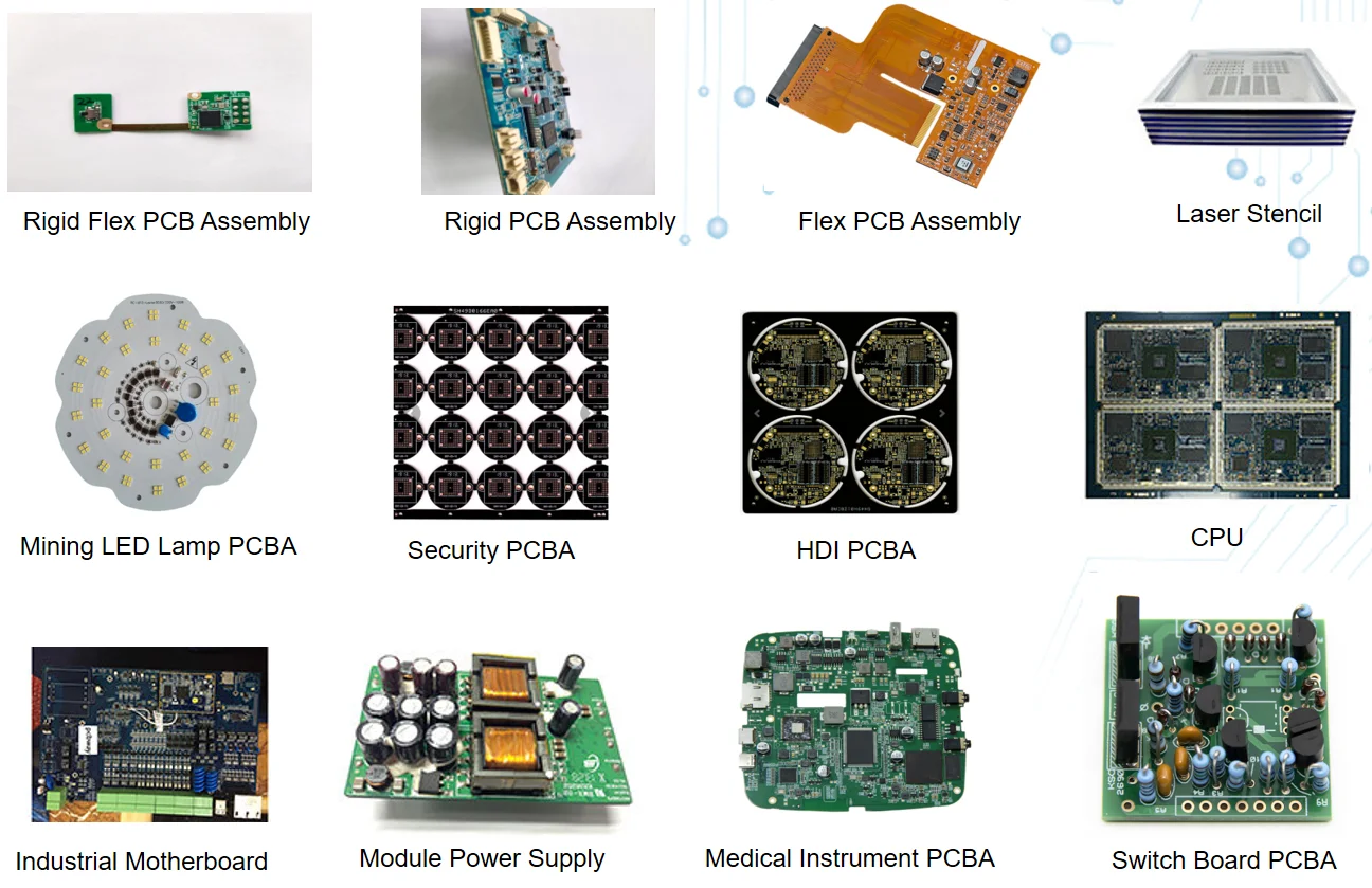
Application
Related Products
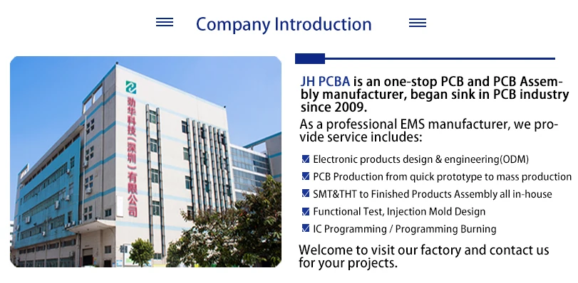
Company Information
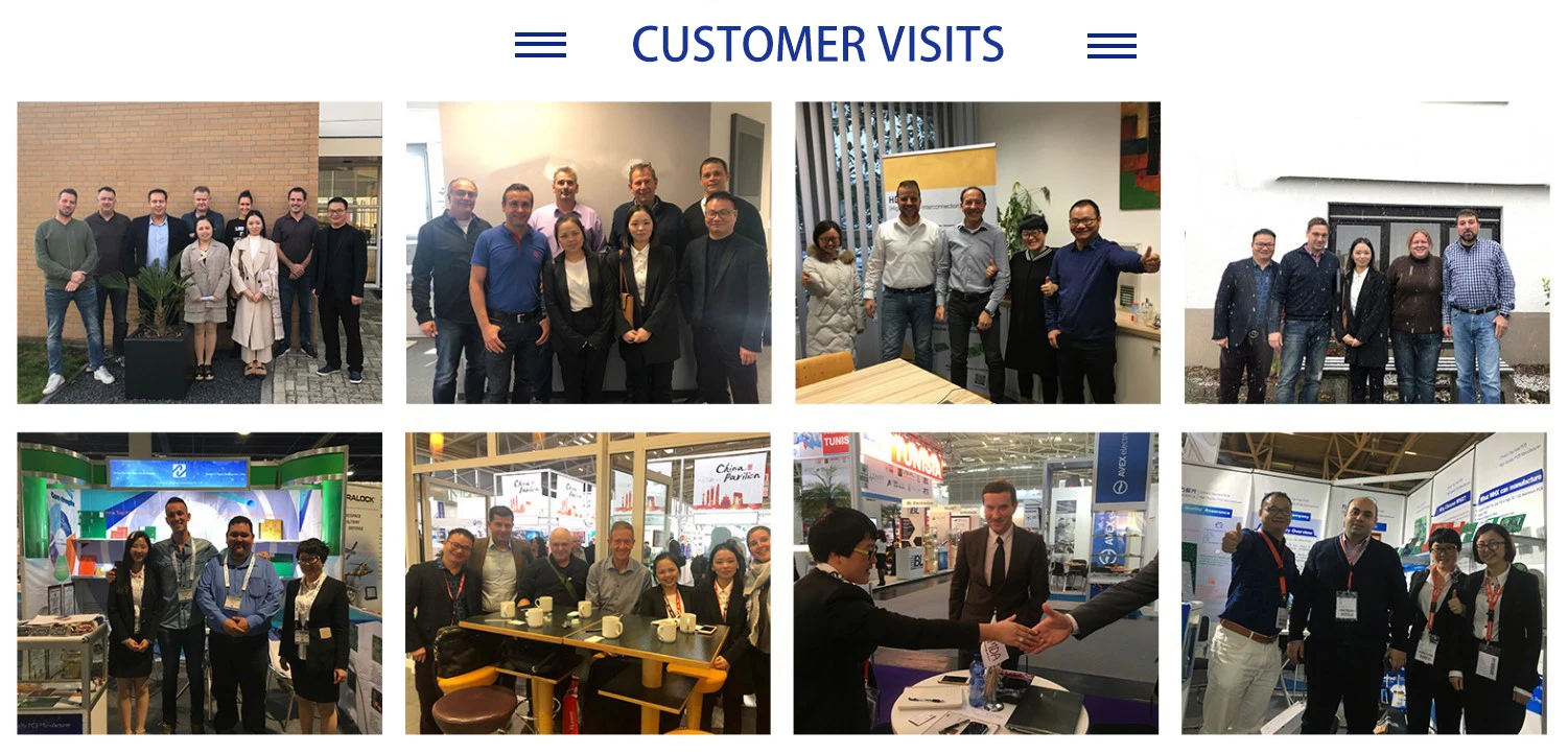
Exhibition
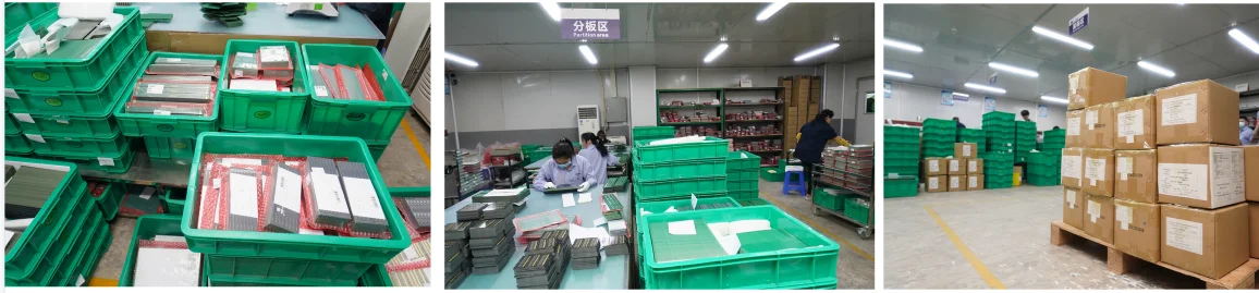
Packaging
Bubble package, EPE package, ESD Bag,Vacuum bag
FAQ
Q1. What does Jinhua Tecenology can do?
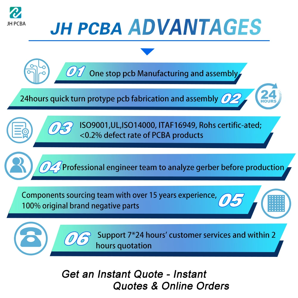
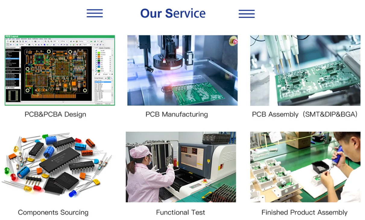
We can support you PCB Design, PCB board manufacturing, Components or Parts Source, Surface Mount (SMT), Thru-Hole (THT),hybrid of both, Functional Test, Wire Soldering etc one stop PCB&PCBA service
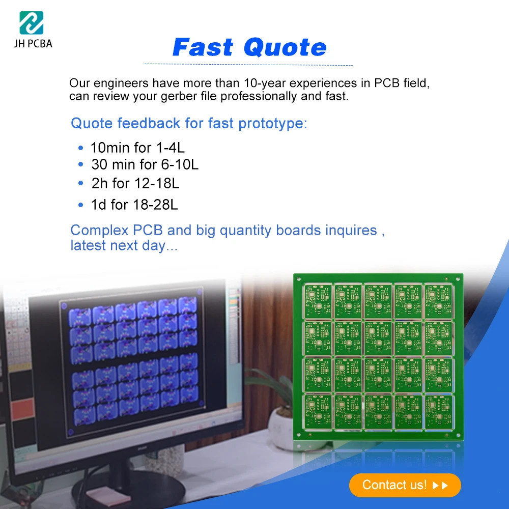
Q2. For PCB quotation, what files format do JINHUA need?
Gerber, Protel 99SE, DXP, PADS 9.5, AUTOCAD, CAM350 are OK.
| Bare PCB Prototype | |
| Layer | Quick Turn |
| 2 | 24 hours |
| 4 | 48 hours |
| 6-8 | 72 hours |
Q3. What will I get from you? Are my files safe?
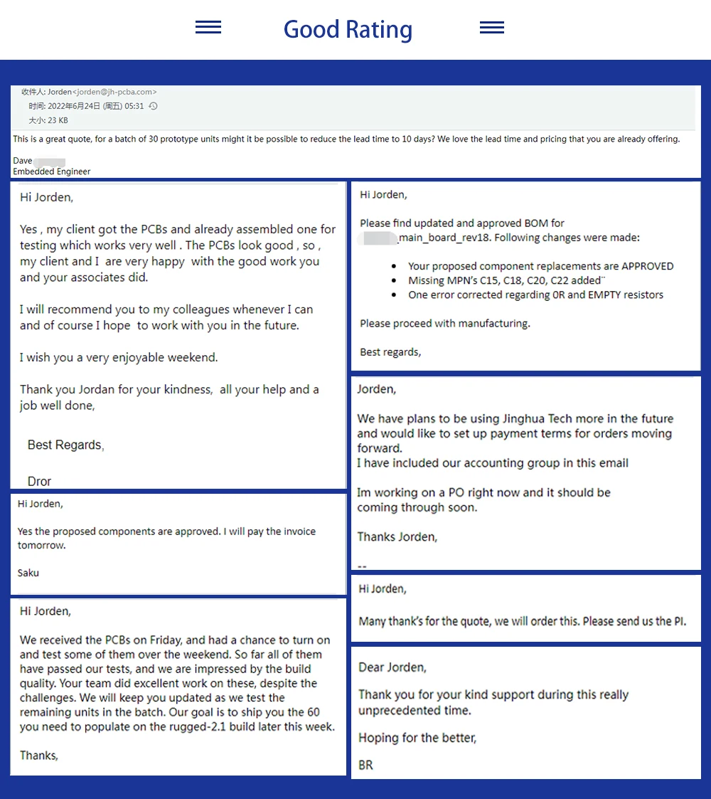
You will get the free DFM feedback for PCB gerber files, BOM list components feedback, Quotation feedback within 2 hours. NDA can be signed for extra security issue.
We Recommend
New Arrivals
New products from manufacturers at wholesale prices