
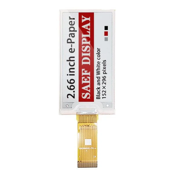
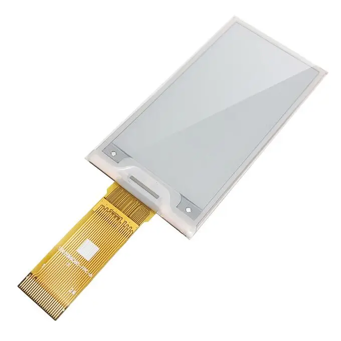
Digital Electronic Shelf Label ESL E ink E paper Display 2.66 Inch 152x296 Dots 3 Colors E Ink Panel
- Category: >>>
- Supplier: Shenzhen Saef Technology Ltd.
Share on (1600592012004):
Product Overview
Description
Product Description
Item of general information | Contents |
Screen Size | 2.66 inche ink display |
Display Mode | Active Matrix EPD |
Display Resolution | 152(H)×296(V) Pixels |
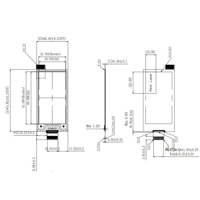
Active Area | 60.088(H) x 30.704(V) mm |
PIN number | 24-pin |
PixelConfiguration | Rectangle |
Outline Dimension | 71.82(H) x 36.3(V) x 1.0(T) mm |
Pixel Pitch | 0.203 x 0.202 (125dpi) |
Logic supply voltage | 3.0V typical |
Operation Temperature | 0°C to +35°C |
Storage Temperature | -25°C to +60°C |
Interface | SPI |
Compliance | REACH & RoHS Compliant |

Product performance description
Found in 2007, SAEF TECH is an experienced LCD/LCM manufacturer. With good quality, professional service and competitive price, we
have been qualified by many well-known companies around the world. SAEF's main advantages that distinguish us from other LCD
vendors are as below: (1) Professional team that have accumulated rich experiences in design/mfg/quality control. (2) Flexible in
biz to support both big and small qty projects from customers. (3) Long product lifetime and Constant Quality product.
3 colors EPD 2.66 inch Screen, 2.66" E-ink ESL Display Description
SAEF Technology SFEPD213BWR-7018A01 is a 3-Colors 2.66” a-Si, active matrix TFT, Electronic Paper Display (EPD) panel. The panel has such high resolution (125dpi) that it is able to easily display fine patterns. Due to its bi-stable nature, the EPD panel requires very little power to update and needs no power to maintain an image.
Features
1. a-Si TFT active matrix Electronic Paper Display(EPD)
2. Three colors support: White, Black, Red
3. Resolution: 296 x 152
4. Ultra-low power consumption
5. Super Wide Viewing Angle - near 180°
6. Extra thin & light
7. SPI interface
8. RoHS compliant
1. a-Si TFT active matrix Electronic Paper Display(EPD)
2. Three colors support: White, Black, Red
3. Resolution: 296 x 152
4. Ultra-low power consumption
5. Super Wide Viewing Angle - near 180°
6. Extra thin & light
7. SPI interface
8. RoHS compliant
Application
Electronic Shelf Label System
Pin Definition
Pin1, NC Not connected
Pin2, GDR / O / Power MOSFET Driver control, this pin is the N-Channel MOSFET Gate Drive Control.
Pin3, RESE / I / Booster Control Input, this pin is the Current Sense Input for the Control Loop.
Pin4, NC Do not connect with other NC pins
Pin5, VSH2 / C / Capacitor. This pin is the Positive Gate driving voltage and the Power Supply pin for VSH2 A stabilizing
capacitor should be connected between VSH2 and GND.
Pin6, NC Not connected
Pin7, NC Not connected
Pin8, BS1 / I / VSS, This pin is setting panel interface.
Pin9, BUSY / O / Device Busy Signal, This pin is Busy state output pin. When Busy is High, the operation of the chip should not be
interrupted, and Command should not be sent.
Pin10, RES# / I / System Reset, This pin is reset signal input. Active Low.
Pin11, D/C# / I / This pin is Data/Command control
Pin12, CS# / I / This pin is the chip select.
Pin13, SCL / I / Serial communication clock input.
Pin14, SDA / I / Serial communication data input/output.
Pin15, VDDIO / P / Power for interface logic pins& I/O. It should be connected with VCI.
Pin16, VCI / P / Power Supply for the chip
Pin17, GND / P / Ground
Pin18, VDDD / C / Internal regulator output A capacitor should be connected between VDD and GND.
Pin19, VPP / P / Power Supply for OTP Programming
Pin20, VSH / C / This pin is the Positive Source driving voltage. A stabilizing capacitor should be connected between VSH and GND.
Pin21, VGH / C / A stabilizing capacitor should be connected between VGH and GND.
Pin22, VSL / C / This pin is the Negative Source driving voltage and the Power Supply pin for VCOM. A stabilizing capacitor should
be connected between VSL and GND.
Pin23, VGL / C / A stabilizing capacitor should be connected between VGL and GND.
Pin24, VCOM / C / This pin is the VCOM driving voltage A stabilizing capacitor should be connected between VCOM and GND.
Typical Operating Sequence
MCU Interface selection In this module , there are 4-wire SPI and 3-wire SPI that can communicate with MCU. The MCU interface mode
can set by hardware selection on BS1 pins. When it is “Low ”,4-wire SPI is selected. When it is “High”,3-wire SPI(9 bits SPI) is
selected.
MCU Serial Interface (4-wire SPI) The 4-wire SPI consists of serial clock SCL, serial data SDA,D/C#,CS#,In SPI mode,D0 acts as
SCL, D1 acts as SDA.
MCU Serial Interface (3-wire SPI) The 3-wire serial interface consists of serial SCL,serial data SDA and CS#. In 3-wire SPI
mode,D0 acts as SCL ,D1 acts as SDA,The pin D/C# can be connected to an external ground. The operation is similar to 4-wire serial
interface while D/C# pin is not used. There are altogether 9-bits will be shifted into the shift register on every ninth clock in
sequence: D/C# bit , D/C bit, D7 to D0 bit,The D/C# bit (first bit of the sequential data )will determine the following data byte
in shift register is written to the Display Data RAM(D/C# bit =1 ) or the command register (D/C# bit = 0 ). Under serial mode ,
only write operations are allowed.
Precaution
(1) The EPD Panel / Module is manufactured from fragile materials such as glass and plastic, and may be broken or cracked if
dropped. Please handle with care. Do not apply force such as bending or twisting to the EPD panel.
(2) It is recommended to assemble or install EPD panels in a clean working area. Dust and oil may cause electrical shorts or
degrade / scratch / dent the protection sheet film.
(3) Do not apply pressure to the EPD panel in order to prevent damaging it.
(4) Do not connect or disconnect the interface connector while the EPD panel is in operation.
(5) Please support the bezel with your finger while connecting the interface cable such as the FPC.
(6) Do not stack the EPD panels / Modules. (7) Do not press the FPC on the glass edge or Pull FPC up / down to 90°.
(8) Do not touch the FPC lead connector.
(9) Do not touch IC bonding area. It may scratch TFT lead or damage IC function.
(10) Wear a Wrist Strap (Grounding connect) when handling and during assembly. Semiconductor devices are included in the EPD Panel
/ Module and they should be handled with care to prevent any electrostatic discharge (ESD). (An Ion Fan may be needed in assembly
operation to reduce ESD risk.)
(11) Keep the EPD Panel / Module in the specified environment and original packing boxes when storage in order to avoid scratching
and keep original performance.
(12) Do not disassemble or reassemble the EPD panel.
(13) Use a soft dry cloth without chemicals for cleaning. Please don’t press hard for cleaning because the surface of the
protection sheet film is very soft and without hard coating. This behavior would make dent or scratch on protection sheet.
(14) Please be mindful of moisture to avoid its penetration into the EPD panel, which may cause damage during operation.
(15) It’s low temperature operation product. Please be mindful the temperature different to make frost or dew on the surface of
EPD pan
Related Products


We Recommend

New Arrivals
New products from manufacturers at wholesale prices


