
Custom Far IR Silicon Si Wafer Crystals High Quality Silicon Wafer Window Plate
- Category: Optical Filters >>>
- Supplier: Huizhou Xinnuo Precision Optics Co. Ltd.
Share on (1600616993577):
Product Overview
Description
Products Description
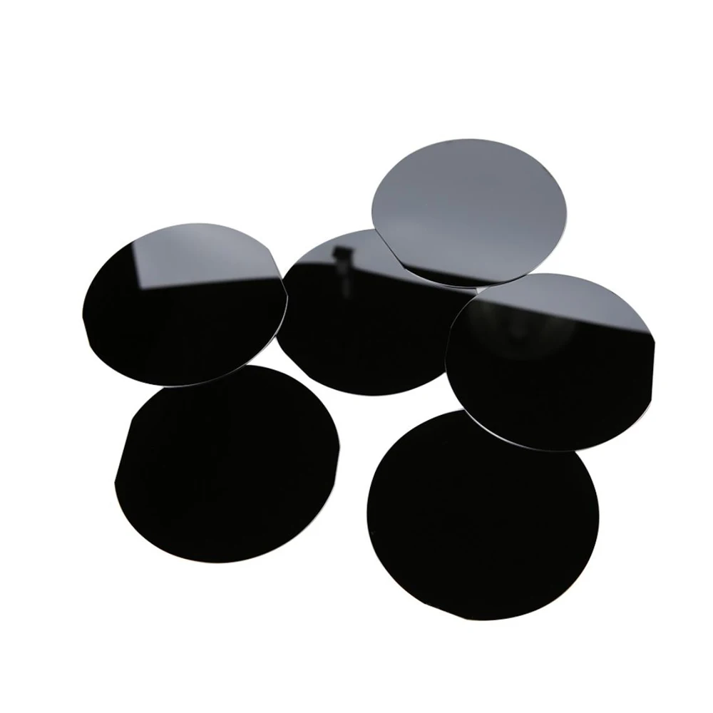
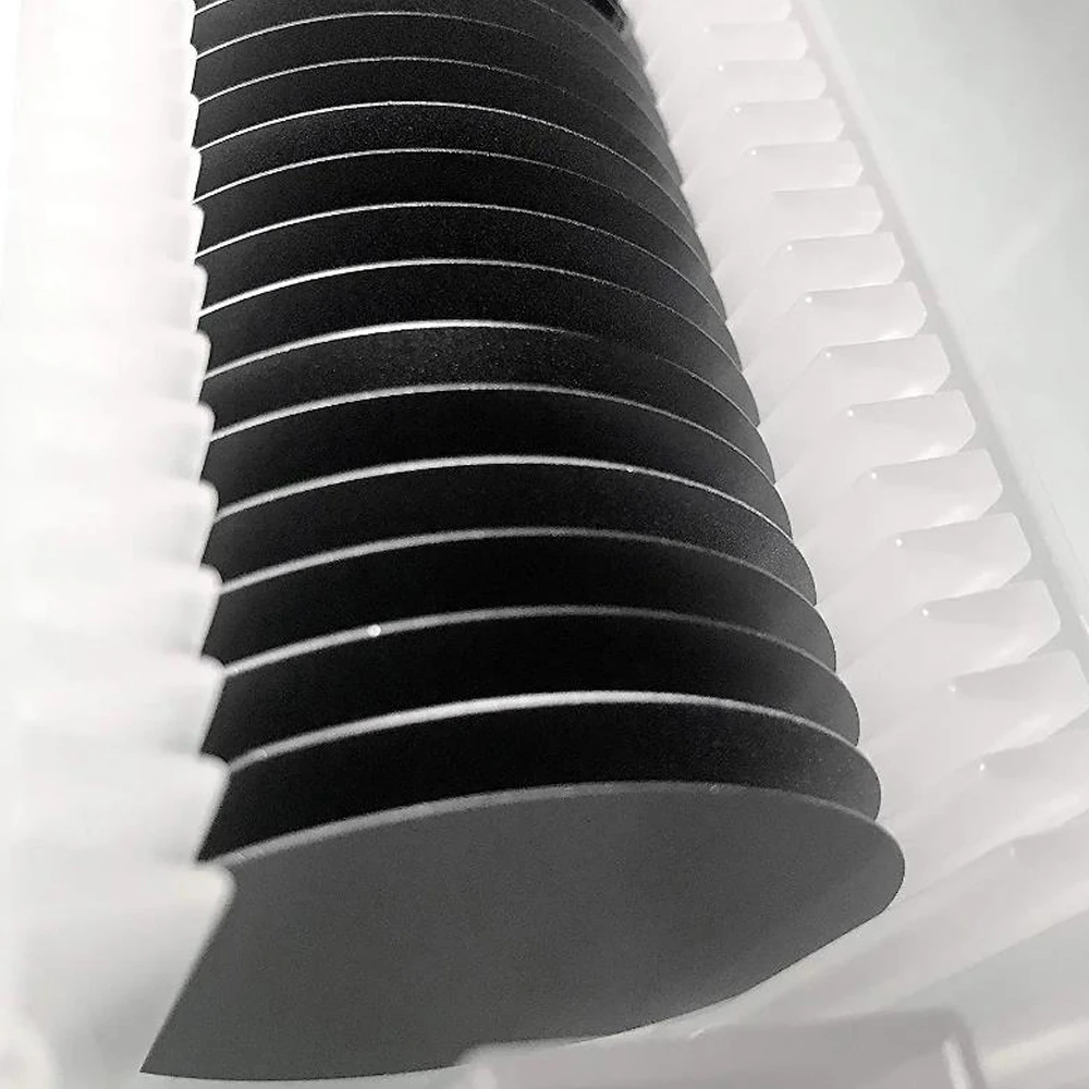
Product Name | Far IR Silicon Wafer |
Material | Si LP5.5um |
Crystal form | N |
Resistivity | 5-40 Ω |
Crystal orientation | 111 |
Specification | Φ4in、6in、8in,Or cut into small pieces |
Center thickness | 0.5mm |
Transmittance | 6-14um Tavg>85% |
Features | Various crystals are widely used in medium wave infrared detectors and infraredthermal imagers, among which silicon (SI) and germanium (GE) are the most widely used infrared optical materials. They have thecharacteristics of metallic luster, hard and brittle, high refractive index, small dispersion, opaque in visible light band, butgood transmittance in infrared band (3 ~ 5um).Due to the small proportion, light weight and high transmittance of monocrystallinesilicon in the middle wave infrared optical system, Si is widely used as the material of optical lens and infrared window in theoptical system. |

Company Profile


Huizhou XinNuo Precision Optics Co.,Ltd was founded in 2013,It is an optical lens coating processing enterprise integrating R&D, design, production, processing and sales.We firmly believe in the concept of win-win cooperation.Over the years, we have made full use of our superb professional knowledge, based on innovation, guided by customer market needs, and focused on the core needs of customers,we provide high grade products, mature technical support ,efficient consultative services based on the principles of focus, integrity and dedication.We are committed to create core value for our customers, do a good job in every product and service.
We mainly produce optical lens coating processing, high grade camera filters and cinema filters (UV Filters, UV-cut, IR-cut, polarizing filters, Graduated Neutral Density Filter, Light reduction ND neutral density filters, magnetic filters ...), mobile phone photography additional function lens, DJI drone additional function filter, industrial lens, camera lens, touch screen panel glass, smart wearable panel, smart switch panel and other products.
We mainly produce optical lens coating processing, high grade camera filters and cinema filters (UV Filters, UV-cut, IR-cut, polarizing filters, Graduated Neutral Density Filter, Light reduction ND neutral density filters, magnetic filters ...), mobile phone photography additional function lens, DJI drone additional function filter, industrial lens, camera lens, touch screen panel glass, smart wearable panel, smart switch panel and other products.
PATENT AND CERTIFICATE
Awarded a number of invention patents,passed ISO9001and other patent certificates in the world.


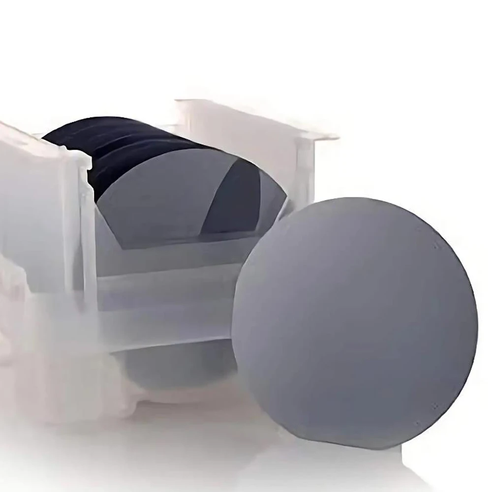
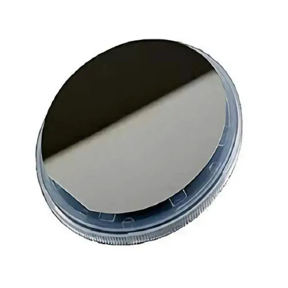
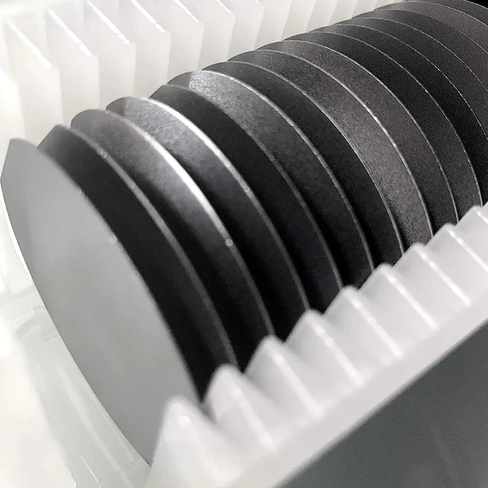
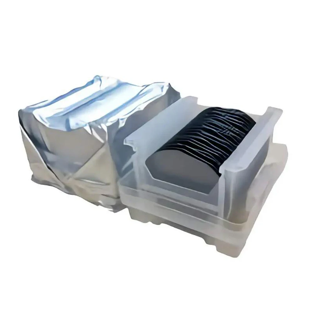
Packing & Delivery

FAQ
Q1: What products can I get from your company?
A: Colored optical glass, optical protection windows, bandpass filter, photography filters etc.
Q2: What's the MOQ?
A: For stocks, no MOQ. For customized colored glass and coating glass, pls contact us for more details.We accept small sample testing order .
Q3: Can I customize the products based on my need?
A: Yes, we can customize the material, specifications and optical coating for your optical components based on your needs.
Q4: What's the delivery time?
A: For inventory: the delivery is within 7 days after you place the order.
B: For customized products: the delivery is 1 or 2 workweeks after you place the order.
Q5:What's the delivery method?
A:Urgent and small order are recommended for Express shipment, such as TNT, DHL, FedEx, UPS etc.
B: Heavy and big orders are recommended for sea shipment. Nominated shiping agent and our own shipping agent are both available.
Contact us
Contact:Jill
Whatsapp/Mobile:+86 13536851425
Email:xn-JillKang@opticfilters.com
Huizhou Xinnuo Precision Optics Co.,Ltd
Building E, Hongtaiyuan Industrial Area, Maan Town, Huicheng District, Huizhou City, Guangdong,China
We Recommend


New Arrivals
New products from manufacturers at wholesale prices


