
Solutions OEM ODM Multilayer Alumina Ceramic PCB Printed Circuit Board Rapid Prototype Individual Ceramic OEM Electronics 1pcs
- Category: >>>
- Supplier: Jinhua Technology (shenzhen) Co. Ltd.
Share on (1600772826581):
Product Overview
Description
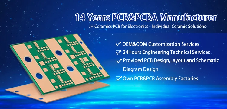
Why choose us?
Our company has advanced processing equipments for ceramic circuit boards. It has the ability to integrate with international technology in the process of laser drilling, cutting, metallization of ceramics, electroplating and thickening of ceramics, through-hole electroplating and filling holes, fabrication of micro-circuits, etc.
Our Advantages:
1.High thermal conductivity
2. Excellent insulation performance
3. Extremely low coefficient of expansion
4. Lower dielectric constant and loss
5. Chemical Corrosion Resistance
Product Description
| JH PCBA Production Capalibity | ||
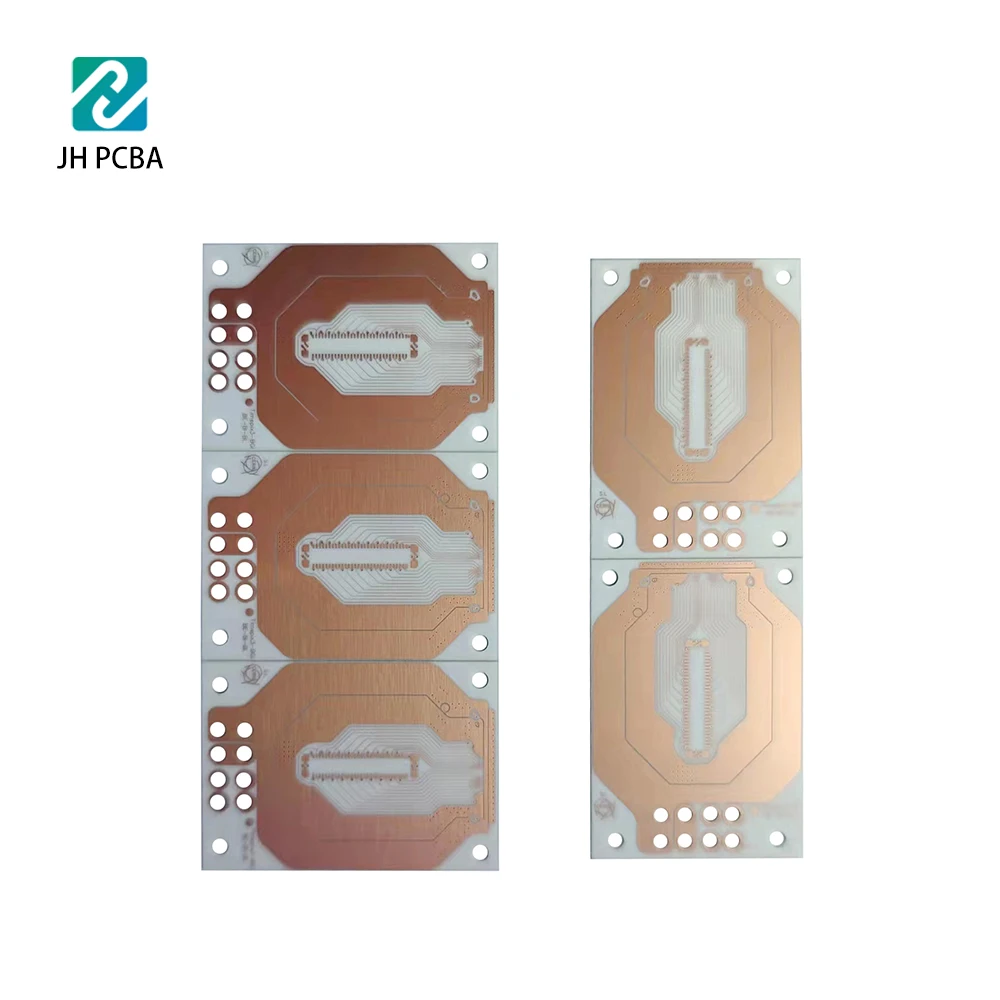
| 1 | Items | Ceramic Substrate |
| 2 | Substrate | Aluminium oxide, Aluminium nitride |
| 3 | Conductor thk | 10-210um |
| 4 | Thermal conductivity | Al203,20-24W/M.k;ALN, 170-220 W/M.k |
| 5 | Reflection | normal: 85-92%, high:≥93% |
| 6 | Surface finiching | Ni/Au, chem.AG, OSP etc. |
| 7 | Panel size | 101.6*101.6mm, 114.3*114.3mm, 120*120mm, 130*140mm, 140*190mm |
| 8 | Board thickness | Min.0.38mm, Max. 2.0mm |
| 9 | Min hole size | 0.08mm |
| 10 | Outline tolerance | ±0.1mm |
| 11 | Peel strength | No broken trace at E poine, gold wire≥7g |
| 12 | Dielectric constant | 9-10@1MHz |
| 13 | Dielectric Strength | ≥2KV |
| 14 | Lead time | 3-5 days for prototype, 7-10 days for production |
| 15 | Inspection standard | MIL-SID-105, class2, AOL=0.65 |
| Layer | Quick Turn/Usual Time | Mass Production |
| 2L | 24 hours/4-5 days | 8-10 days |
| 4L | 48 hours/6-7 days | 10-12 days |
| 6L | 72 hours/7-8 days | 12-14 days |
| 8L | 72 hours/8-10 days | 16-18 days |
| 10L | 96 hours/12-14 days | 18-20 days |
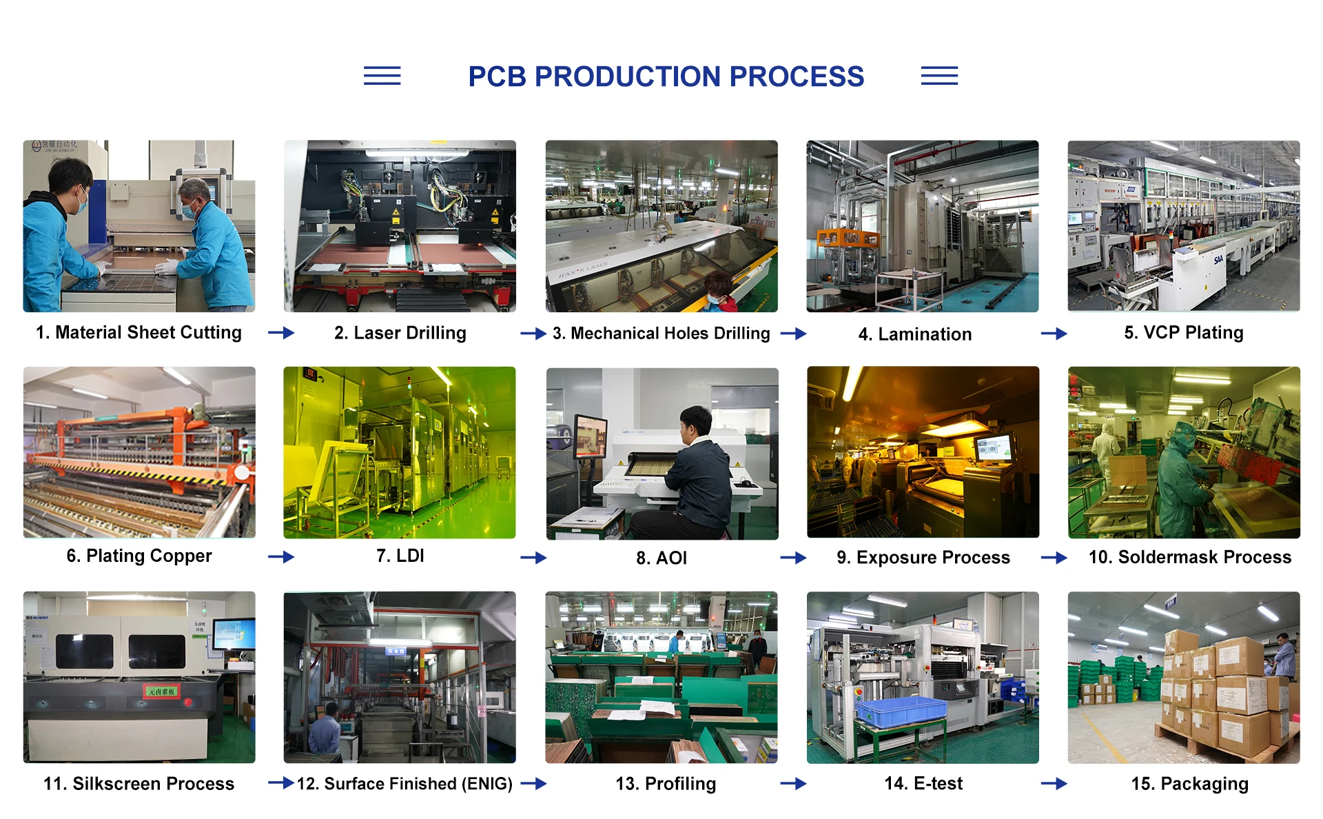
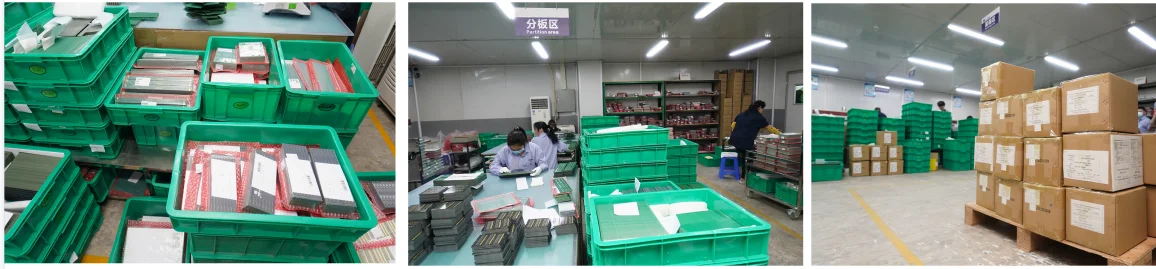
Production Process
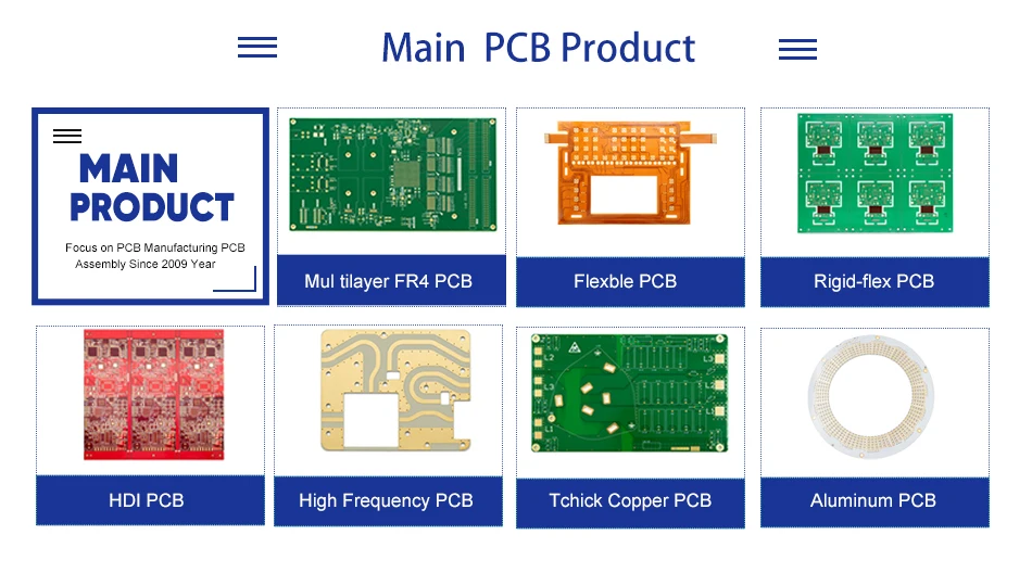
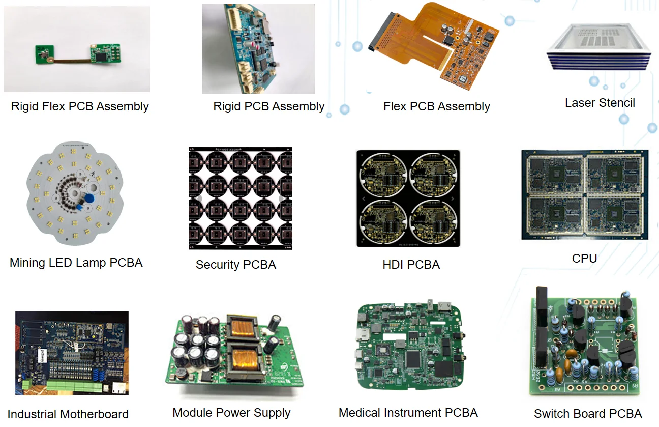
Related Products
Company Information
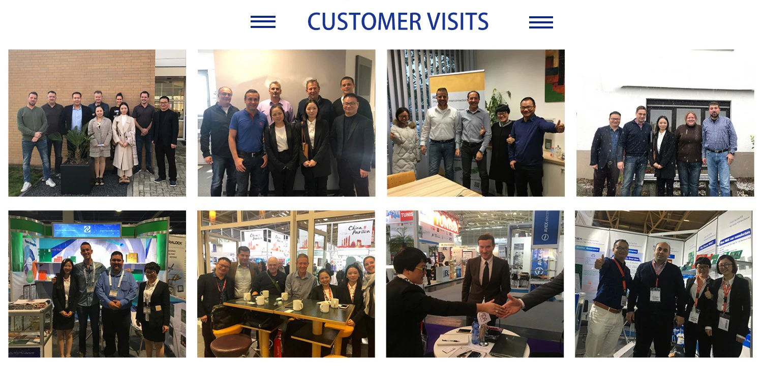
Exhibition
Packaging
Bubble package, EPE package, ESD Bag,Vacuum bag
FAQ
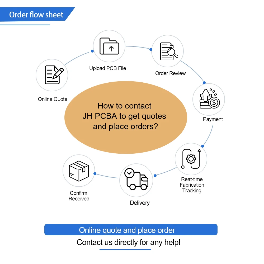
Q1. What does Jinhua Tecenology can do?
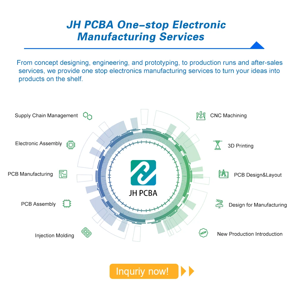
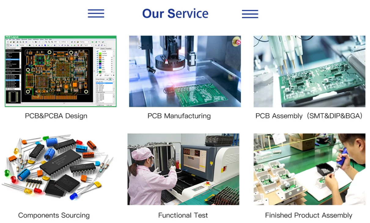
We can support you PCB Design, PCB board manufacturing, Components or Parts Source, Surface Mount (SMT), Thru-Hole (THT),hybrid of both, Functional Test, Wire Soldering etc one stop PCB&PCBA service
Q2. For PCB quotation, what files format do JINHUA need?
Gerber, Protel 99SE, DXP, PADS 9.5, AUTOCAD, CAM350 are OK.
| Bare PCB Prototype | |
| Layer | Quick Turn |
| 2 | 24 hours |
| 4 | 48 hours |
| 6-8 | 72 hours |
Q3. What will I get from you? Are my files safe?
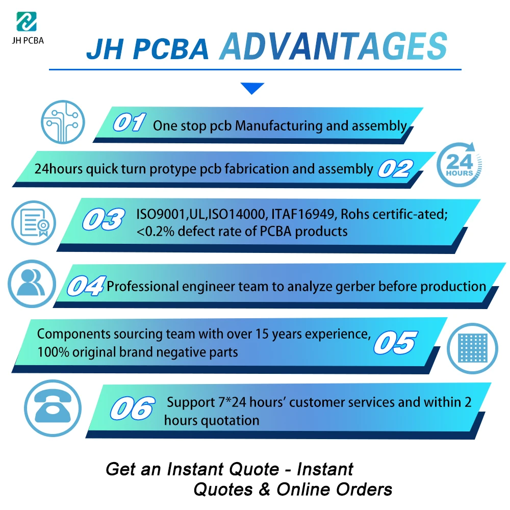
You will get the free DFM feedback for PCB gerber files, BOM list components feedback, Quotation feedback within 2 hours. NDA can be signed for extra security issue.
We Recommend
New Arrivals
New products from manufacturers at wholesale prices