
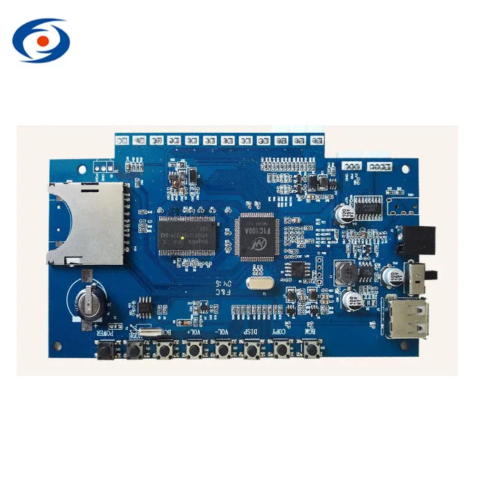
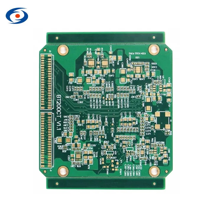
One Stop Pcb Prototype Circuit Board And Assembly Double Sided PCB
- Category: >>>
- Supplier: Shenzhen Yytimes Electronics Co. Ltd.
Share on (1600792965348):
Product Overview
Description
Products Description
Layers | 4 layers |
Board Thickness | 1.6mm |
Material | Fr4 |
Copper Thickness | 35um |
Size | Customization |
Number of Layers | 1,2,4,6,up to 32layers |
PCB Standard | IPC-A-610 D/IPC-III Standard |
Surface Finish | HASL LEAD FREE |
Testing Service | AOI X-Ray Function Test |
Certificate | ISO9001/Iso14001/CE/ROHS |
Inner package | Vacuum packing |
Board Thickness Tolerance | ±0.1mm |
Min. Hole Size | 0.1mm |
Min. Line Width/Gap | 0.075mm |
Impedance | Customization |
MOQ | 1pc |

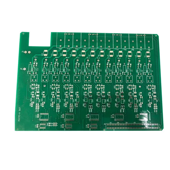
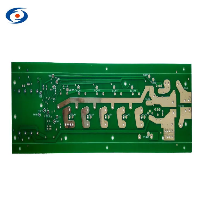
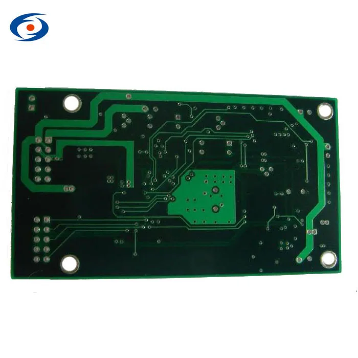
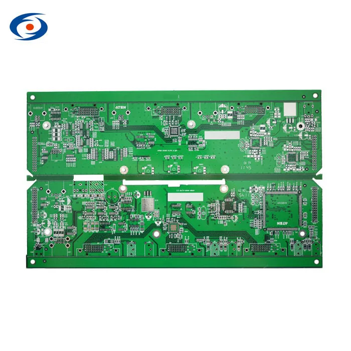
Picture


FR4 PCB Technical Capacity | ||||
Item | Capability | Details | ||
PCB layers | 1-32 layers PCB | |||
Material | FR-4 (Standard FR4, Mid-Tg FR4,Hi-Tg FR4, Lead free assembly material) , Halogen-Free, Ceramic filled , Teflon, Polyimide | |||
Max size | 560x1100mm | normal size within 550x420mm | ||
Outline tolerance | ±0.05mm / ±0.1mm | CNC tolerance ±0.1mm,V-cut board outline tolerance±0.05mm | ||
PCB thickness | 0.4--3.2mm | 0.4/0.6/0.8/1.0/1.2/1.6/2.0/2.4/3.0/3.2mm | ||
PCB thickness tolerance | ±0.1mm | |||
Surface Finish | HASL/HALS LeasFree/OSP/ENIG/Hard Gold/Golden finger | |||
Min trace width | 3mil(0.075mm) | |||
Min trace distance | 3mil(0.075mm) | |||
Finished outer layer copper thickness | 35um/70um/105um(1OZ/2OZ/3OZ) | the finished PCB's outer layer copper thickness,1 OZ=35um,2 OZ=70um, 3OZ=105um | ||
Finished inner layer copper thicknss | 35um/50um | For prototype, inner copper thickness is 50um | ||
Drill size ( machine drill) | 0.2--6.3mm | 0.2mm is the minmum drill size, 6.3mm is the maxmum drill size the machine can drill. | ||
Via annular ring | ≥0.153mm(6mil) | Minimum size of via annular ring can not be less than 0.153mm | ||
Finished TH size ( machine drill) | 0.2--6.20mm | Size of Finished hole is usually smaller than size in drill file because it has copper attahced. | ||
Hole tolerance (machine drill ) | ±0.08mm | Hole tolerance is ±0.08mm, for a designed 0.6mm hole,finished hole size will be between 0.52--0.68mm. | ||
Type of solder resist | Liquid photoimagable solder mask (LPSM) | |||
Minimum Silscreen character Width | ≥0.15mm | Other wise it will be not clear for visual | ||
Minimum Silscreen character Length | ≥0.8mm | Other wise it will be not clear for visual | ||
Character width to height ratio | 1:05 | Best width to height ratio for silkscreen printing. | ||
Distance from trace to outline | ≥0.3mm(12mil) | For routing,distance from trace to outline should ≥0.3mm;For V-cut this distance should be ≥0.4mm | ||


SMT MACHINE | ||||
ITEM | YAMAHA F8S | YAMAHA G5SD | ||
Machine Size | 1.2m*2.8m | 1.2m*2.8m | ||
Capacity | 12500CPH | 7500CPH | ||
Components Size | 0.3*0.15mm-44*44mm | 0.3*0.15mm-72*72mm | ||
Components Thickness | MAX.12.7mm | MAX.25.4mm | ||
Pin Spacing | ≥0.3mm | ≥0.3mm | ||
Min. Pin Width | 0.1mm | 0.1mm | ||
Min.Pin Length | 0.2mm | 0.2mm | ||
BGA Dia. | 0.13mm | 0.13mm | ||
BGA Spacing | 0.25mm | 0.25mm | ||
Type of Component | MAX.80 | MAX.80 | ||
PCBA Technical Capacity | ||
Quantity | Prototype & Batch | |
Type of Assembly | SMT,Thru-hole | |
Solder Type | Water Soluble Solder Paste,Leaded and Lead-Free | |
Components | Passive Down to 01005 size | |
BGA and VFBGA | ||
Leadless Chip Carriers/CSP | ||
Double-sided SMT Assembly | ||
Fine Pitch to 0.8mils | ||
BGA Repair and Reball | ||
Part Removal and Replacement | ||
File Formate | Bill of Materials | |
Gerber files | ||
Pick-N-Place file | ||
Types of Service | Turn-key,partial turn-key or consignment | |
Component package | Cut Tape,Tube,Reels,Loose Parts | |
Testing | Flying Probe Test,X-ray Inspection AOI Test | |
PCBA certification | UL Approval,ROHS,ISO9001:2000,TS16949 | |

Company Profile


One-Stop Service


Our Advantages

Customer Feedback

FAQ
1.How long have you been in business?
YH Circuit: We have been supplying printed circuit boards since 2002.
2.What cetificates do you have?
YH Circuit: We have been ISO9001/IATF16949/UL.
3.How long will it take to get a quote?
YH Circuit: We return domestic quotes the same day, usually within hours. Offshore quotes are generally returned within 24 hours.
4.Do you handle PCB quick turnaround?
YH Circuit: We specialize in quick turns. We can turn 1-2layers boards in one day, for 4-6layers pcb we build them in 3-5 days.
5.What happens if the design changes while in process?
YH Circuit: We are quite resourceful and may be able to incorporate the changes in process. If the changes are too drastic, we will be forced to restart the order.
6: Are my files safe?
YH Circuit:: Your files are held in complete safety and security.We protect the intellectual property for our customers in the whole process.. All documents from customers are never shared with any third parties. We are willing to sign NDA effect by customer side local law and promising to keep customers data in high confidential level.
7.What payment methods you accept?
YH Circuit:
* T/T
* Western Union (little wire transfer cost for small amount)
* L/C
* PayPal
* Other Methods
Product packaging


We Recommend
New Arrivals
New products from manufacturers at wholesale prices


