
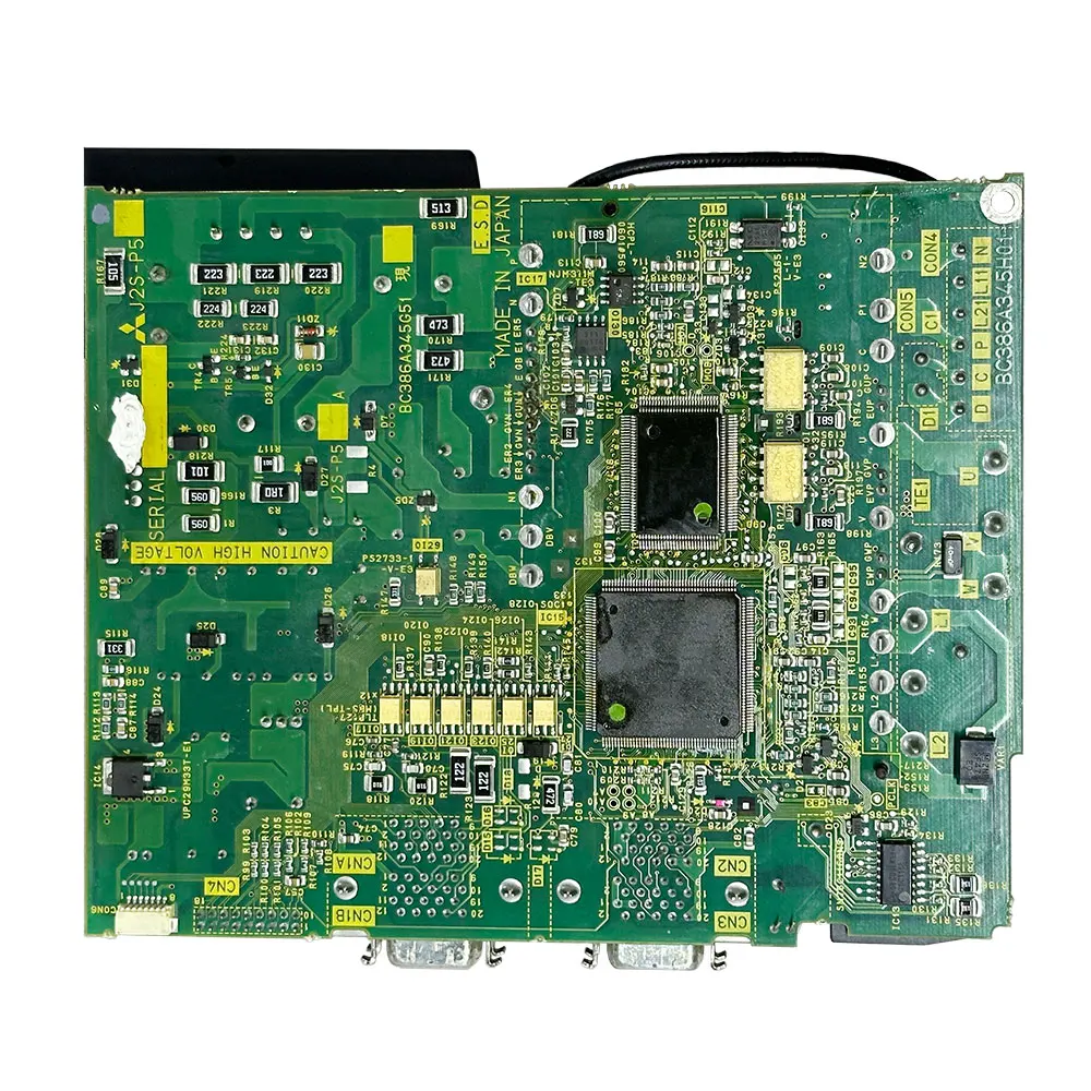
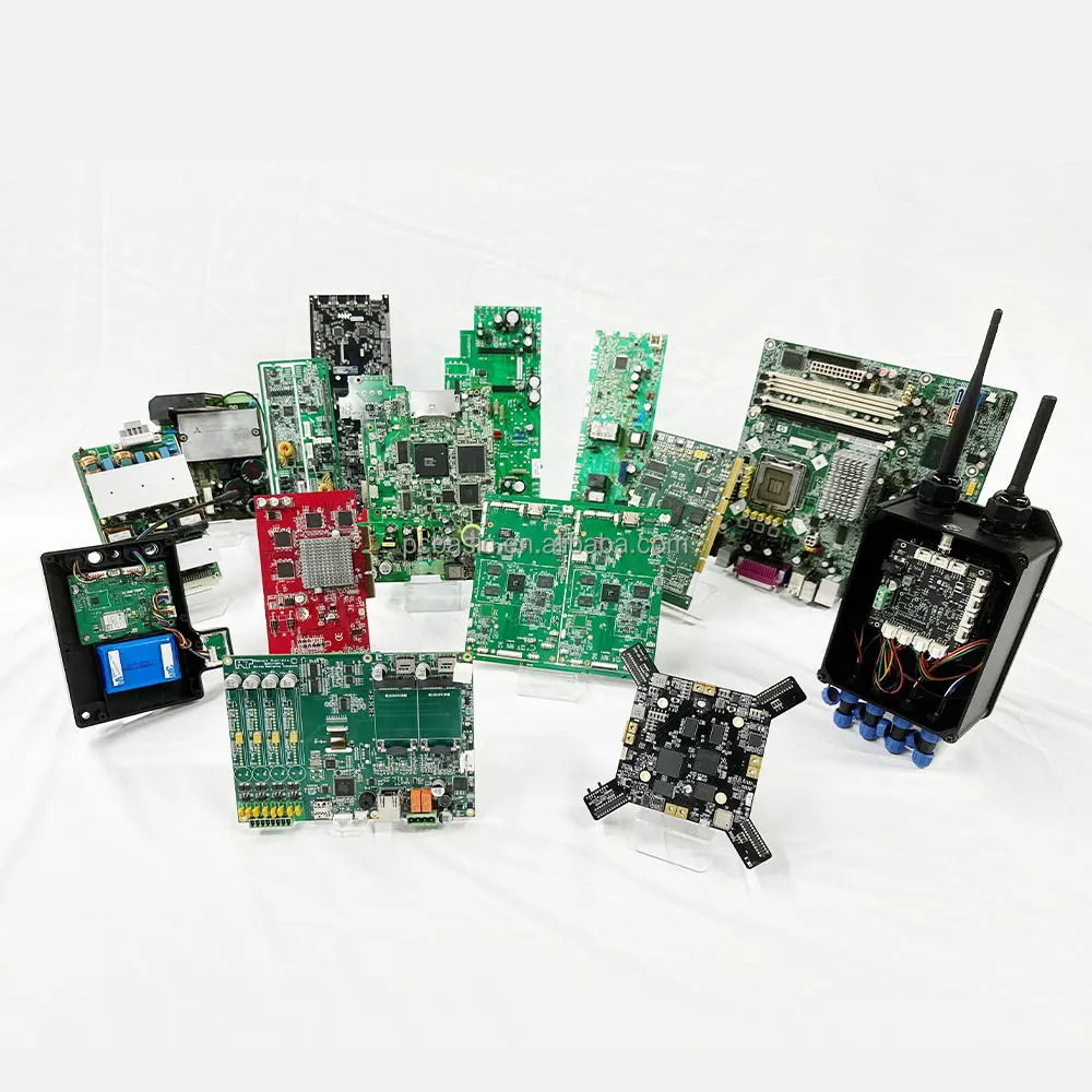
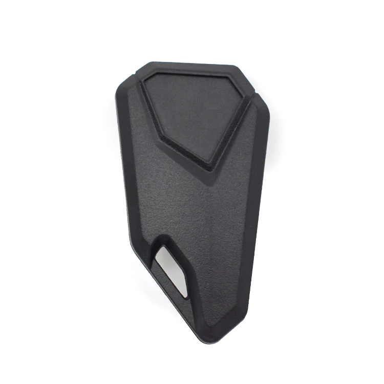
Smart Electronics OEM One Stop Service Double Sided Pcb Pcb Amplifier For Wifi Radio Receiver Internet Radio Pcb Board
- Category: >>>
- Supplier: Shenzhen JS Technology Co. Ltd.
Share on (1600829171180):
Product Overview
Description

Company Profile

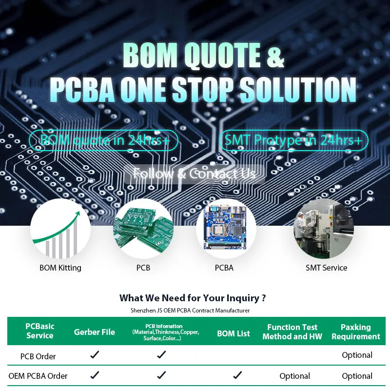
PCBabsic is a professional PCBA manufacturer with 13 years of production experience. We specialize in one-stop fast production of multi-variety small batch R&D, PCBA to finished product assembly. We have 8 fully automatic SMT patch production lines, 1 DIP wave production line, and multiple post-welding assembly production lines. Equipped with a series of high-precision automated production equipment and quality control systems to ensure thatour product quality is always stable and reliable.
Ourunique advantages: Confidential and Nondisclosure Agreement: We protect the lntellectual Property for our customers in the whole process. Our staff of trained professionals are all working under a strict confidentiality contract and keep the business secrets.
Flexibility: Customers-oriented. We forever center on customers' demands, constantly update and introduce into technology, fully understand customers' requirements and offer our professional suggestion.
Flexibility: Customers-oriented. We forever center on customers' demands, constantly update and introduce into technology, fully understand customers' requirements and offer our professional suggestion.


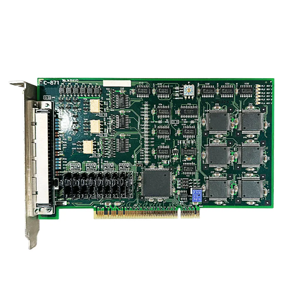
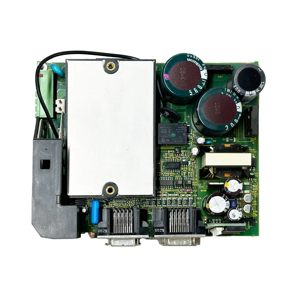
Product Details
-
PCB Assembly Capability | ||
Item | Capability | |
PCB Base Material | FR-4/ High TG FR-4/ Aluminum/ Ceramic/ Copper/ Halogen Free material/ Rogers/ Arlon/ Taconic/ Teflon | |
PCB Layers | 1-40 | |
Copper Thickness | 1-6OZ | |
Finished Board Thickness | 0.2-7.0mm | |
Min Hole Size | Mechanical hole: 0.15mm Laser hole: 0.1mm | |
Surface Treatment | HASL, HASL lead free, Immersion Gold, Immersion Tin, lmmersion Silver, Hardgold, Flash gold, OSP... | |
Outline Profile | Rout/ V-cut/ Bridge/ Stamp hole | |
Advantages | ----Intelligent Management System, Intelligent Factory | |
----Professional Surface-mounting and Through-hole soldering technology | ||
----Various sizes like 1206,0805,0603 components SMT technology | ||
----ICT(In Circuit Test),FCT(Functional Circuit Test) | ||
----PCB Assembly With IPC,CCC,FCC,Rohs Approval | ||
----High Standard SMT&Solder Assembly Line | ||
----High density interconnected board placement technology capacity. | ||
Quantity | Prototype & Low Volume PCB Assembly,from 1 Board to 100, or up to 1000 and customized | |
Type of Assembly | SMD, Through-hole, and mixed Assembly | |
Solder Type | Water Soluble Solder Paste, Leaded and Lead-Free | |
File Formate | Gerber files, Pick-N-Place file, Bill of Materials | |
Component packaging | Cut Tape,Tube,Reels,Loose Parts | |
Testing | Flying Probe Test,X-ray Inspection AOI Test, High-Low Temperature Testing, Drop Testing, Salt Spray Testing, Vibration Testing | |
Turn Time | Same day service to 15 days service | |
PCB assembly process | Drilling----Exposure-----Plating-----Etaching & Stripping---Punching-----Electrical Testing-----SMT-----Wave Soldering-----Assembling---- ICT-----Function Testing-----Temperature & Humidity Testing | |
Lead Time | ||
PCB Assembly Proofing | 24 Dours | |
PCB Assembly 100 sets | 2-3 Days | |
PCB Assembly 1000 sets | 3 -5 Days | |


Why Choose Us


More About Us


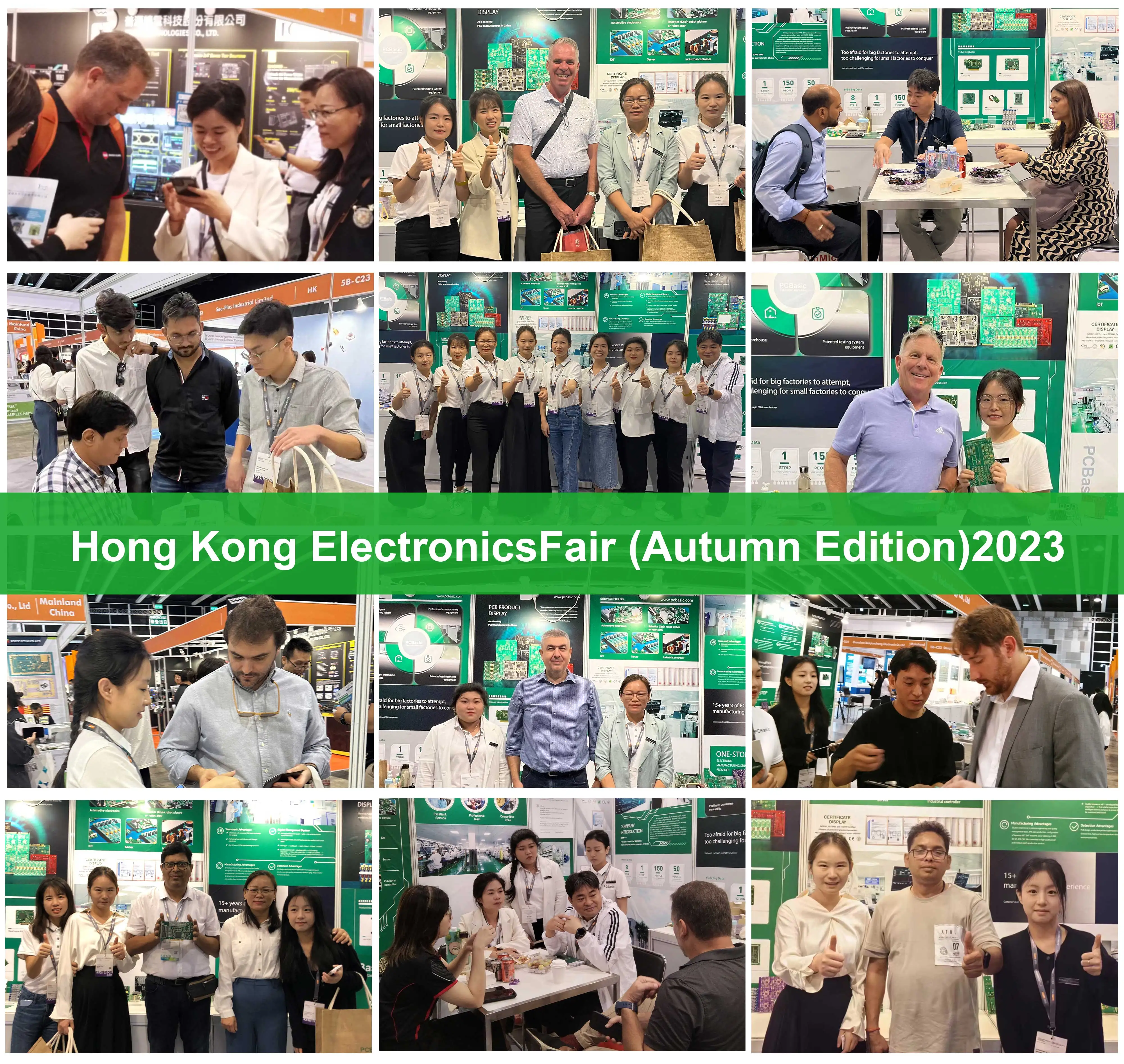
Customers And Exhibitions


PCB Assembly Process


Certificates And Customer Feedback


FAQ
Q: What type of services do you provide ?
PCBasic: We provide turnkey solutions including PCB fabrication, components sourcing, SMT/DIP assembly, testing, mold injection, and other value-added services.
Q: What is required for PCB & PCBA quotation?
PCBasic:
1. For PCB: QTY, Gerber filesand technical requirements(material, size, surface finish treatment, copper thickness, board thickness etc).
2. For PCBA: PCB information, BOM list, Testing documents.
Q: What is your minimum order quantity (MOQ)?
PCBasic: No MOQ limited, sample and mass production both support.
Q:Do you keep the provider product information and design files confidential?
PCBasic: We are willing to sign a NDA effect by customers side local law and promising to keep customers data in high confidential level.
Q: Do you accept process materials supplied by clients?
PCBasic: Yes, we can provide component source, and also accept component from client.
Q: Are you factory or a middle man?
PCBasic: Our factory is located in Building E, Jianshi Industrial Park, Shajing, Shenzhen, Guangdong, China.Welcome to visit us.
You are welcome to visit at any time. If you are inconvenient to visit the site due to various circumstances, we will also provide you with an online video introduction at any time.

Our advantages


PCB Assembly Process


Product packaging

Our team


Exhibition

Certificate


FAQ
Q: What type of services do you provide ?
PCBasic: We provide turnkey solutions including PCB fabrication, components sourcing, SMT/DIP assembly, testing, mold injection, and other value-added services.
PCBasic: We provide turnkey solutions including PCB fabrication, components sourcing, SMT/DIP assembly, testing, mold injection, and other value-added services.
Q: What is required for PCB & PCBA quotation?
PCBasic:
1. For PCB: QTY, Gerber filesand technical requirements(material, size, surface finish treatment, copper thickness, board thickness etc).
2. For PCBA: PCB information, BOM list, Testing documents.
PCBasic:
1. For PCB: QTY, Gerber filesand technical requirements(material, size, surface finish treatment, copper thickness, board thickness etc).
2. For PCBA: PCB information, BOM list, Testing documents.
Q: What are the main appkication use cases of your PCB/PCBA services?
PCBasic: Automotive, Medical, Industry Control, IOT, Smart Home, Military, Aerospace etc.、
PCBasic: Automotive, Medical, Industry Control, IOT, Smart Home, Military, Aerospace etc.、
Q: What is your minimum order quantity (MOQ)?
PCBasic: No MOQ limited, sample and mass production both support.
PCBasic: No MOQ limited, sample and mass production both support.
Q:Do you keep the provider product information and design files confidential?
PCBasic: We are willing to sign a NDA effect by customers side local law and promising to keep customers data in high confidential level.
PCBasic: We are willing to sign a NDA effect by customers side local law and promising to keep customers data in high confidential level.
Q: Do you accept process materials supplied by clients?
PCBasic: Yes, we can provide component source, and also accept component from client.
PCBasic: Yes, we can provide component source, and also accept component from client.
Q: Are you factory or a middle man?
PCBasic: Our factory is located in Building E, Jianshi Industrial Park, Shajing, Shenzhen, Guangdong, China.Welcome to visit us.
PCBasic: Our factory is located in Building E, Jianshi Industrial Park, Shajing, Shenzhen, Guangdong, China.Welcome to visit us.
You are welcome to visit at any time. If you are inconvenient to visit the site due to various circumstances, we will also provide you with an online video introduction at any time.

We Recommend
New Arrivals
New products from manufacturers at wholesale prices


