
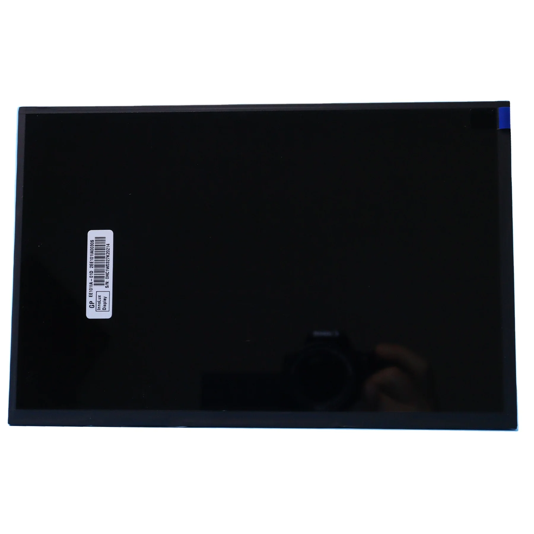
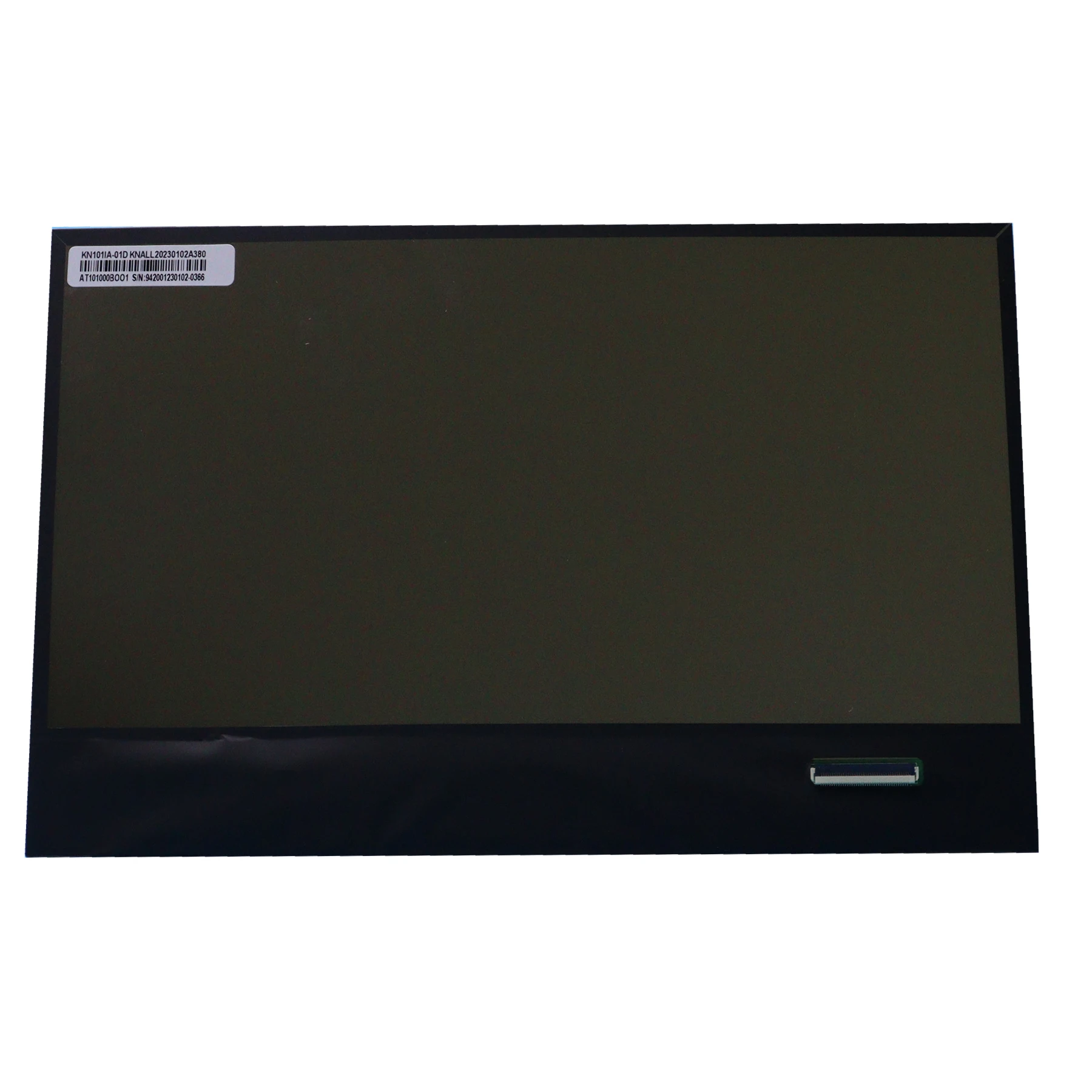
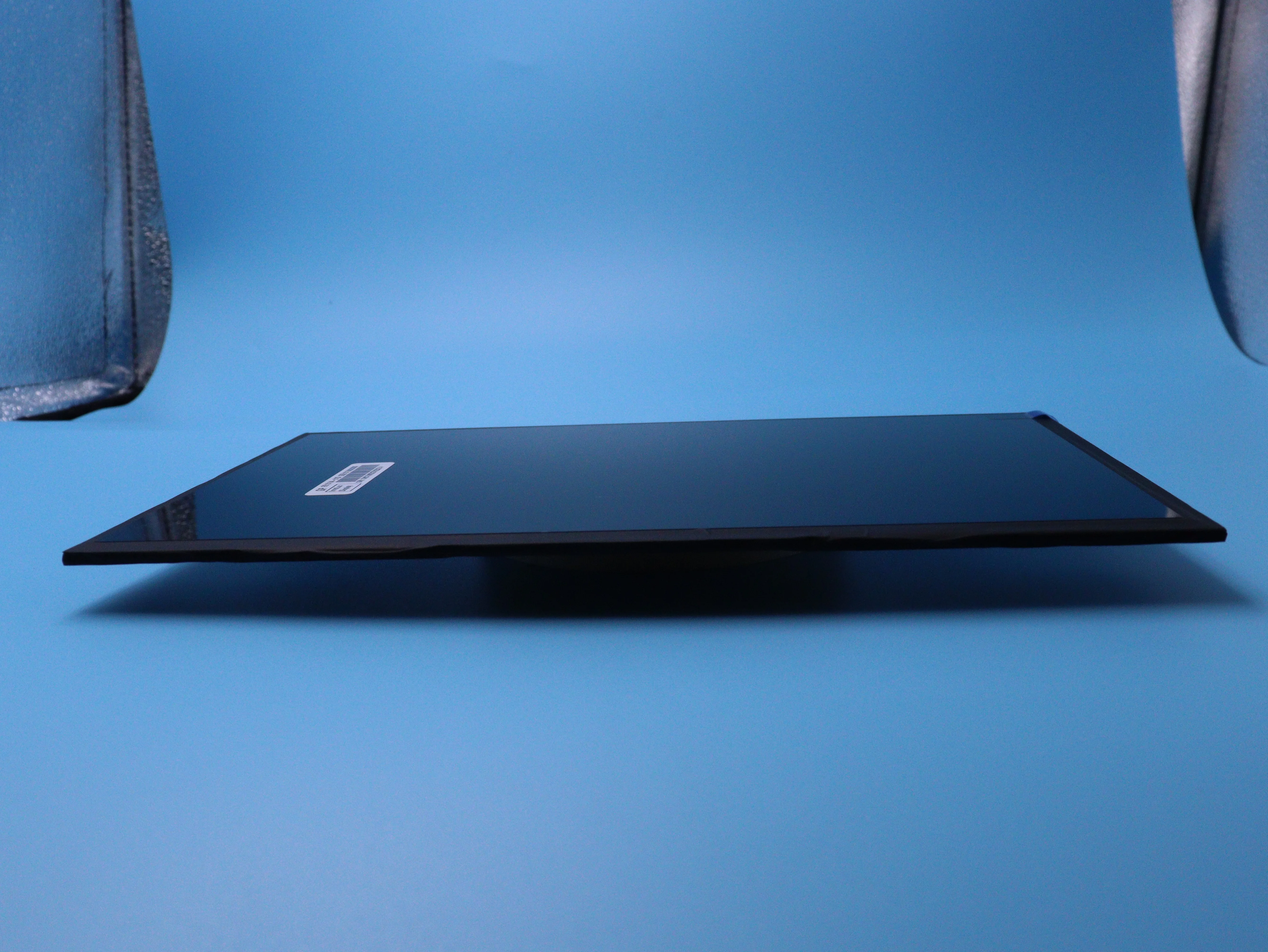
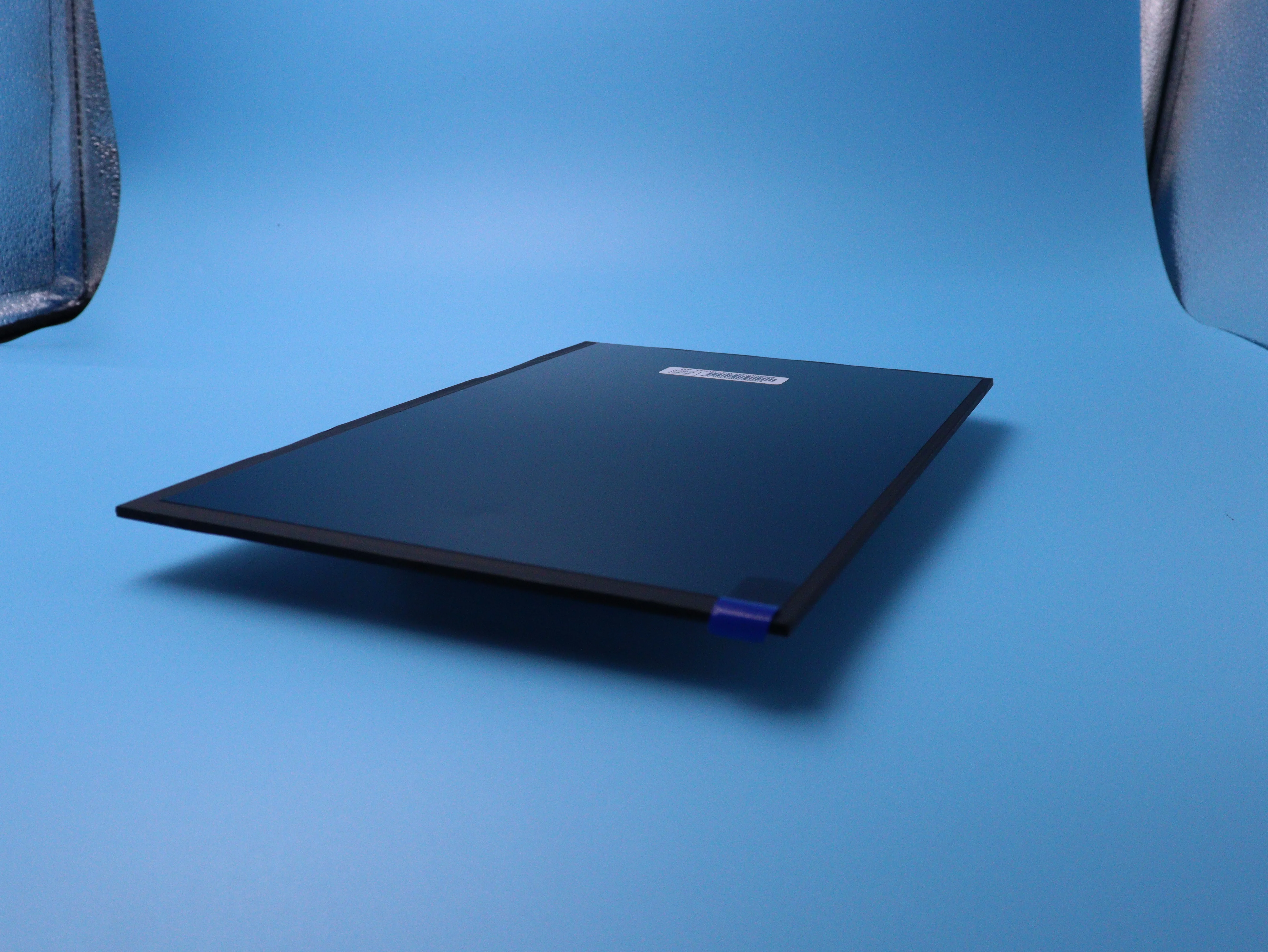
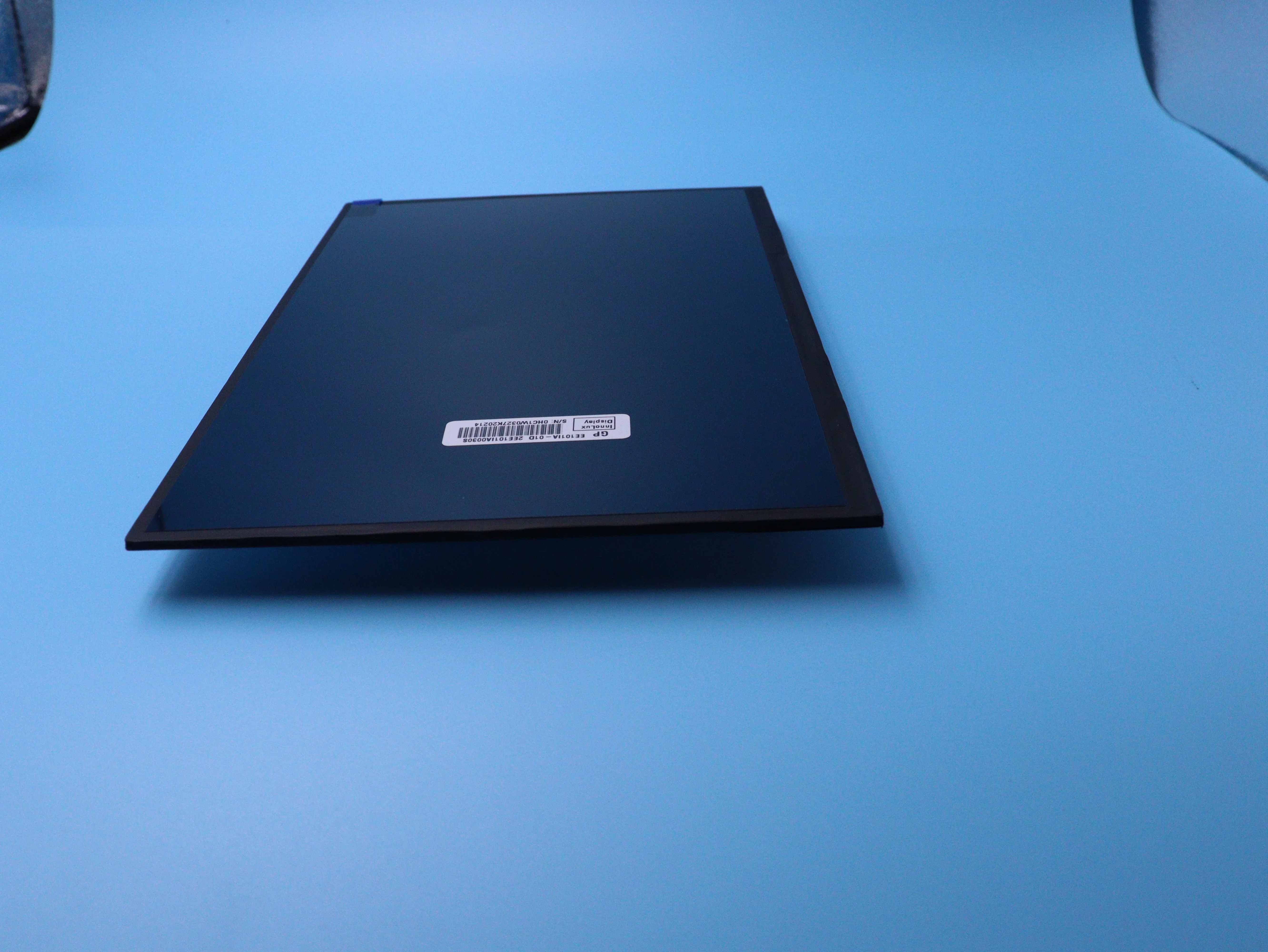
Affordable lcd 10.1 inch touch display LCD Module for 10.1inch lcd 1200 800 10 inchlcd displai 10.1 tft lcm mipi 10 inches round
- Category: >>>
- Supplier: Shenzhen Kanon Photoelectric Co. Ltd.
Share on (1600845654087):
Product Overview
Description


General Specifications | ||||
No. | Item | Specification | ||
1 | LCD size | 10.1 inch(Diagonal) | ||
2 | Driver element | a-Si TFT active matrix | ||
3 | Resolution | 1280 × 3(RGB) × 800 | ||
4 | Display mode | Normally Black, Transmissive | ||
5 | Dot pitch | 0.0565(W) × 0.1695(H) mm | ||
6 | Active area | 216.96(W) × 135.60(H) mm | ||
7 | Panel size | 223.95(W) ×144.24(H) ×1.07(D) mm | ||
8 | Surface treatment | HC | ||
9 | Color arrangement | RGB-stripe | ||
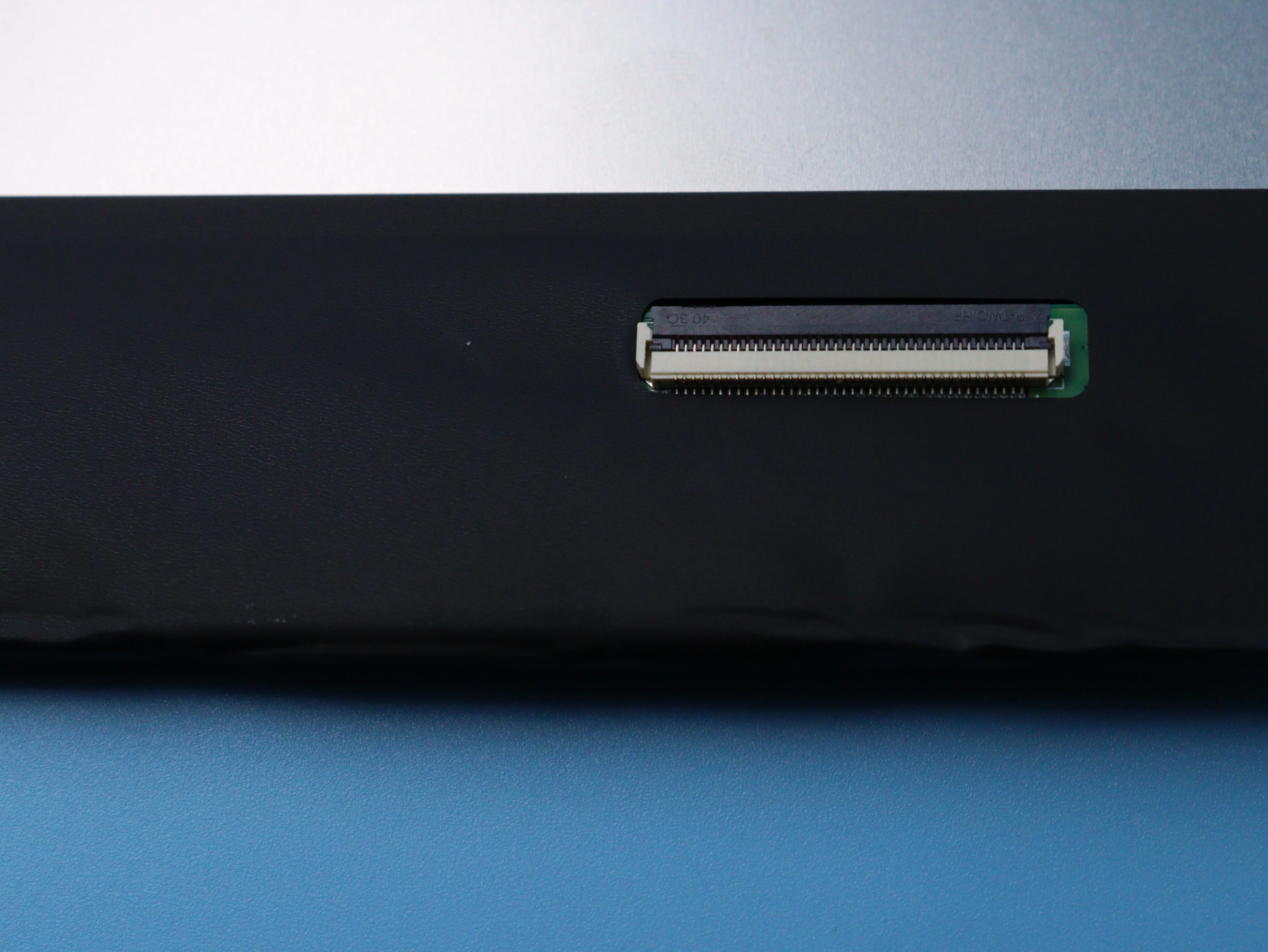
10 | Interface | LVDS | ||
11 | View direction(Gray Inversion) | free | ||
12 | Panel power consumption | 0.307W(typ) | ||
13 | Weight | 80g(Typ) | ||
14 | inversion | column | ||
15 | IC | EK79202 | ||
Pin Assignment | ||||||||
Pin No. | Symbol | I/O | Function | Remark | ||||
1 | NC | --- | No connection | |||||
2 | VDD | P | Power Supply | |||||
3 | VDD | P | Power Supply | |||||
4 | NC | --- | Only for INX test | |||||
5 | NC | --- | Only for INX test | |||||
6 | NC | --- | Only for INX test | |||||
7 | GND | P | Ground | |||||
8 | Rxin0- | I | -LVDS Differential Data Input | R0-R5, G0 | ||||
9 | Rxin0+ | I | +LVDS Differential Data Input | |||||
10 | GND | P | Ground | |||||
11 | Rxin1- | I | -LVDS Differential Data Input | G1~G5, B0,B1 | ||||
12 | Rxin1+ | I | +LVDS Differential Data Input | |||||
13 | GND | P | Ground | |||||
14 | Rxin2- | I | -LVDS Differential Data Input | B2-B5,HS,VS, DE | ||||
15 | Rxin2+ | I | +LVDS Differential Data Input | |||||
16 | GND | P | Ground | |||||
17 | RxCLK- | I | -LVDS Differential Clock Input | LVDS CLK | ||||
18 | RxCLK+ | I | +LVDS Differential Clock Input | |||||
19 | GND | P | Ground | |||||
20 | Rxin3- | I | -LVDS Differential Data Input | R6, R7, G6, G7, B6, B7 | ||||
21 | Rxin3+ | I | +LVDS Differential Data Input | |||||
22 | GND | P | Ground | |||||
23 | NC | --- | No connection | |||||
24 | NC | --- | No connection | |||||
25 | GND | P | Ground | |||||
26 | NC | --- | No connection | |||||
27 | NC | --- | No connection | |||||
28 | NC | --- | No connection | |||||
29 | AVDD | P | Power for Analog Circuit | |||||
30 | GND | P | Ground | |||||
31 | LED- | P | LED Cathode | |||||
32 | LED- | P | LED Cathode | |||||
33 | NC | --- | No connection | |||||
34 | NC | --- | No connection | |||||
35 | VGL | P | Gate OFF Voltage | |||||
36 | NC | --- | No connection | |||||
37 | NC | --- | No connection | |||||
38 | VGH | P | Gate ON Voltage | |||||
39 | LED+ | P | LED Anode | |||||
40 | LED+ | P | LED Anode | |||||
1.1. Absolute Maximum Ratings | ||||||||||
Item | Symbol | Values | Unit | Remark | ||||||
Min. | Max. | |||||||||
Power voltage | VDD | 2.2 | 3.6 | V | ||||||
AVDD | 7.9 | 8.5 | V | |||||||
VGH | 13 | 17 | V | |||||||
VGL | -11 | -15 | V | |||||||
VGH-VGL | 24 | 32 | V | |||||||
Operation Temperature | TOP | -20 | 70 | ℃ | ||||||
Storage Temperature | TST | -30 | 80 | ℃ | ||||||


Copy the information:
Email:admin@szkngd.cn
Tel:+86 13684946095
FB:tanqingjia
Tel:+86 13684946095
FB:tanqingjia


We Recommend


New Arrivals
New products from manufacturers at wholesale prices


