
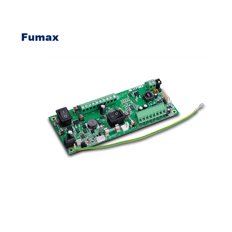
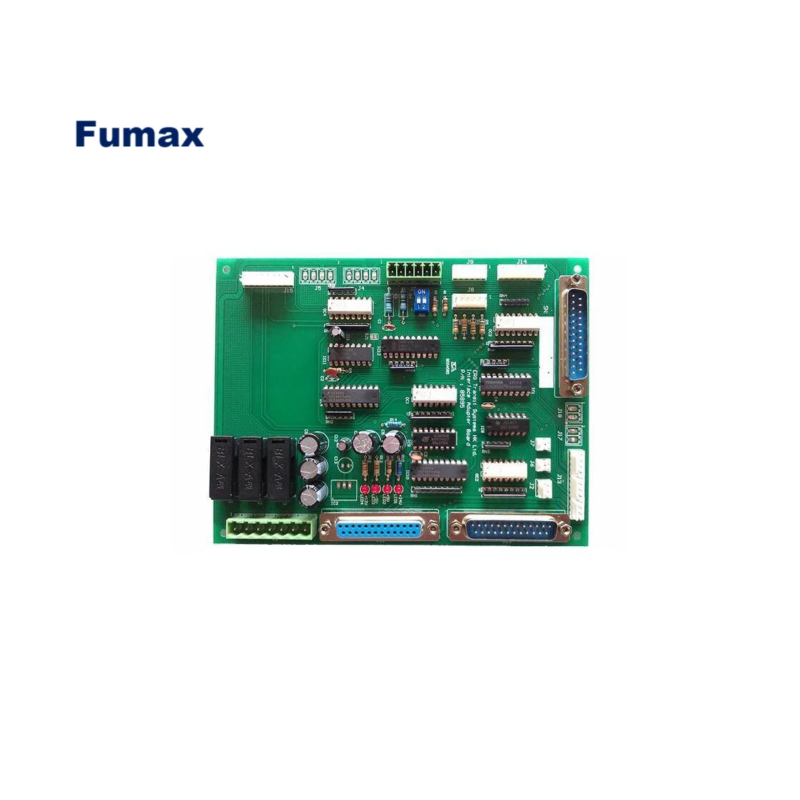
Manufacture Motherboard Parts Processing OEM PCBA PCB Fabrication Factory Electric Equipment Circuit board
- Category: >>>
- Supplier: Shenzhen Fumax Technology Co. Ltd.
Share on (1600935287503):
Product Overview
Description
PCB&PCBA Capability
Products Description

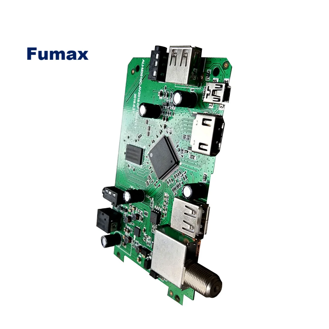
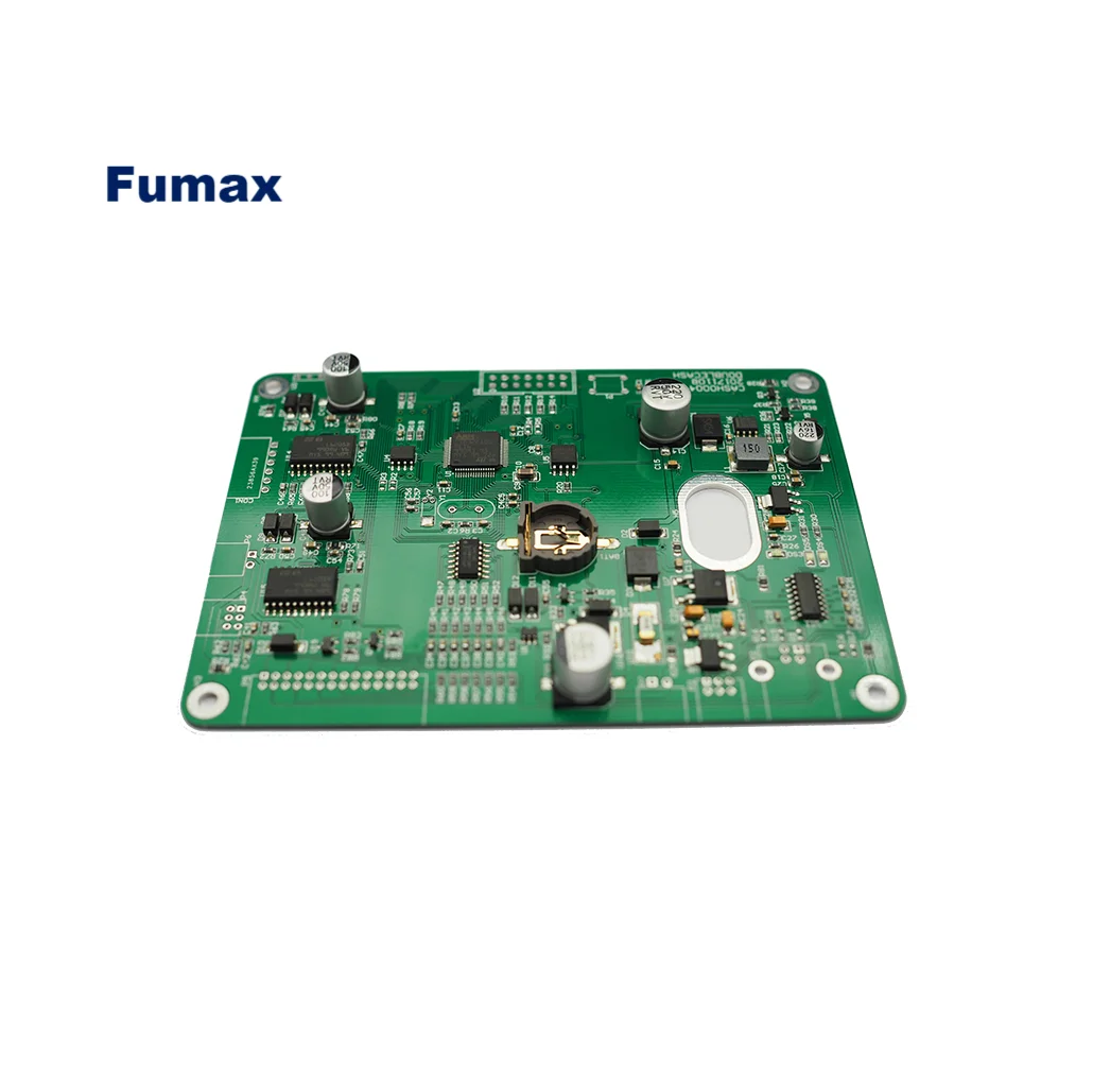
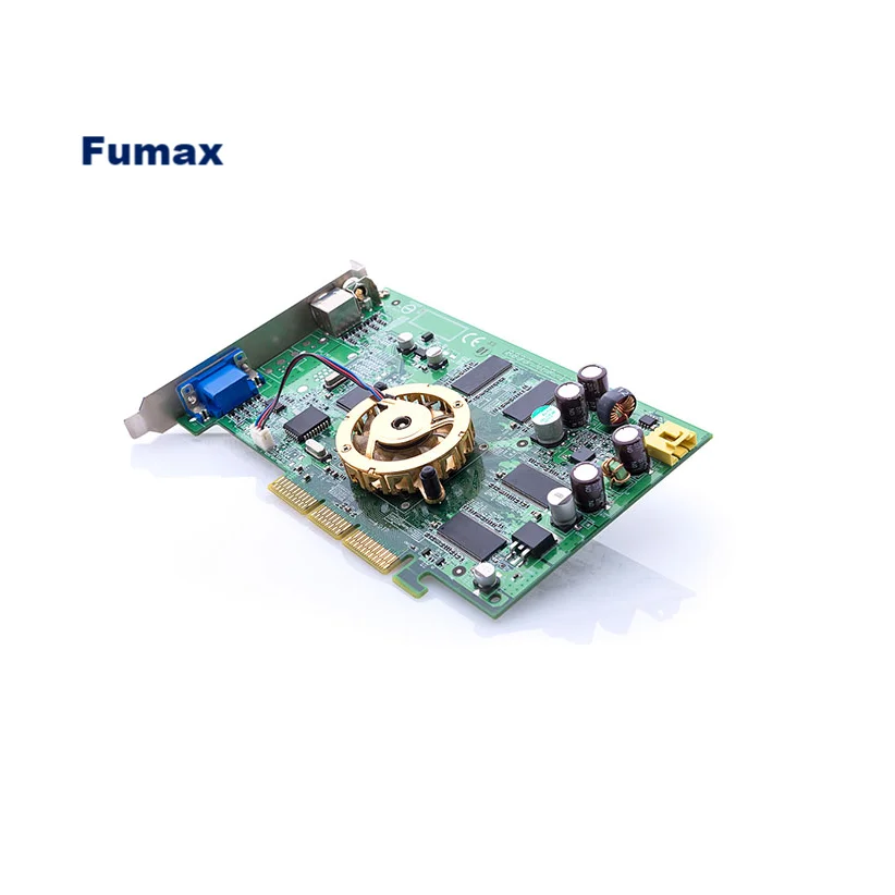
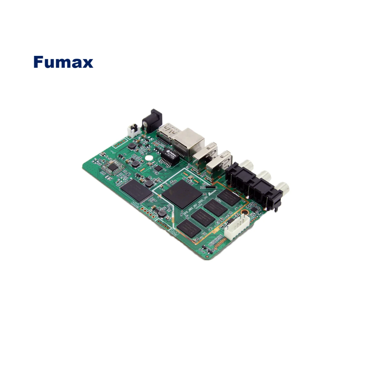
Custom PCBA manufacturer one stop service pcb assembly
From component soucring to final assembly
PCB Capability | PCBA Capability | ||||
Type | Capability | Type of Assembly | SMT (Surface-Mount Technology) | ||
Double Side | CEM-3、 FR-4、Rogers RO4233、Bergquist Thermal Clad 4mil–126mil (0.1mm-3.2mm) | THD (Thru-Hole Device) | |||
Multilayers | 4-28 layers, board thickness 8mil-126mil (0.2mm-3.2mm) | SMT & THD mixed | |||
Buried/Blind Via | 4-20 layers, board thickness 10mil-126mil(0.25mm-3.2mm) | Double sided SMT and THD assembly | |||
HDI | 1+N+1、2+N+2、3+N+3、Any layer | SMT capability | PCB layer: 1-32 layers; | ||
Flex & Rigid-Flex PCB | 1-8layers Flex PCB ,2-12layers Rigid-flex PCB HDI+Rigid-flex PCB | PCB material: FR-4, CEM-1, CEM-3, High TG, FR4 Halogen Free, FR-1, FR-2, Aluminum Boards; | |||
Soldermask Type(LPI) | Taiyo、Goo’s、Probimer FPC..... | PCB thickness: 0.2mm-7.0mm; | |||
HASL/Lead Free HASL | Thickness: 0.5-40um | PCB dimension width: 40-500mm; | |||
Electro-nickel palladium Ni-Au | Au: 0.015-0.075um Pd 0.02-0.075um Ni:2-6umm | Chip accuracy: laser recognition ±0.05mm; image recognition ±0.03mm; | |||
Min Mechanical Drill Hole | 0.20mm | Component size: 0.6*0.3mm-33.5*33.5mm; | |||
Min. Laser Drill Hole | 4mil (0.100mm) | Pin spacing laser recognition over 0.65mm; | |||
Line Width/Spacing | 2mil/2mil | BGA spherical distance: ≥0.25mm; | |||
Max. Panel Size | 21.5" X 24.5"(546mm X 622mm) | BGA Globe distance: ≥0.25mm; | |||
Line Width/Spacing Tolerance | Non electro coating:+/-5um,Electro coating:+/-10um | BGA ball diameter: ≥0.1mm; | |||
PTH Hole Tolerance | +/-0.002inch(0.050mm) | IC foot distance: ≥0.2mm; | |||
NPTH Hole Tolerance | +/-0.002inch(0.050mm) | Component Package | Reels | ||
Hole Location Tolerance | +/-0.002inch(0.050mm) | Cut tape | |||
Hole to Edge Tolerance | +/-0.004inch(0.100mm) | Tube and tray | |||
Edge to Edge Tolerance | +/-0.004inch(0.100mm) | Loose parts and bulk | |||
Layer to Layer Tolerance | +/-0.003inch(0.075mm) | Board Shape | Rectangular | ||
Impedance Tolerance | +/- 10% | Round | |||
Warpage % | Max≤0.5% | Slots and Cut outs | |||
Laser Via Drill/Pad | 0.125/0.30 、 0.125/0.38 | Complex and Irregular | |||
Blind Via Drill/Pad | 0.25/0.50 | Assembly process | Lead-Free (RoHS, REACH) | ||
Line Width/Spacing | 0.10/0.10 | Design File Format | Gerber | ||
Hole Formation | CO2 Laser Direct Drill | BOM (Bill of Materials) (.xls,.CSV, . xIsx) | |||
Build Up Material | FR4 LDP(LDD); RCC 50 ~100 micron | Coordination (Pick-N-Place/XY file) | |||
Cu Thickness on Hole Wall | Blind Hole: 10um(min) | Electrical Testing | AOI (Automated Optical Inspection), | ||
Aspect Ratio | 0.8 : 1 | X-ray Inspection | |||
SMT Assembly patch (Yes/No) | YES | ICT (In-Circuit Test)/ Functional testing | |||
Air Gap capability (Yes/No) | YES | Standard | |||
Production of hard and soft binding plate(Yes/No) | YES | Custom | |||
Our advantage
PCB Fabrication (Rigid and Flex)
PCB Assembly (10 SMT & 8 DIP lines, IPC610 solering)
Complete Assembly (Component sourcing, PCB Assembly and Box building)

Supported Capabilities
Supported Capabilities | |
Types of Assembly | SMT (Surface-Mount Technology) |
THD (Thru-Hole Device) | |
SMT & THD mixed | |
Double sided SMT and THD assembly | |
SMT capability | PCB layer: 1-32 layers; |
PCB material: FR-4, CEM-1, CEM-3, High TG, FR4 Halogen Free, FR-1, FR-2, Aluminum Boards; | |
Board type: Rigid FR-4, Rigid-Flex boards | |
PCB thickness: 0.2mm-7.0mm; | |
PCB dimension width: 40-500mm; | |
Copper thickness: Min:0.5oz; Max: 4.0oz; | |
Chip accuracy: laser recognition ±0.05mm; image recognition ±0.03mm; | |
Component size: 0.6*0.3mm-33.5*33.5mm; | |
Component height: 6mm(max); | |
Pin spacing laser recognition over 0.65mm; | |
High resolution VCS 0.25mm; | |
BGA spherical distance: ≥0.25mm; | |
BGA Globe distance: ≥0.25mm; | |
BGA ball diameter: ≥0.1mm; | |
IC foot distance: ≥0.2mm; |
Our facility
Our Company
Firmware Programming
Function Test
AOI Team
DIP Line
Mold Line
Package
Through Hold Assembly
Wave Soldering Machine
Customized Plastic Available
4 SMT Line (80000 pcs one day)
Safety warehouse
Our Manufacturer Capacity
Coating Process
Our Team‘s Ability
Our Certificate


Contact us

FAQ

Q:Can some core ICs be supplied by customers for PCBA proofing?
A: Yes, we support this model even for mass production.
Q: Can you help me burn the program, test PCBA and then deliver it?
A: Yes, our engineers can help complete MCU burning, program testing and other processes, and then deliver them. If necessary, we can help customers to issue test rack.
A: Yes, we can. We are a professional manufacturer with one-stop turnkey service from component sourcing to final assembly.
Q: Can you produce the goods as customer design?
A: Welcome to send us the design and sample, we will evaluate and feedback you shortly.
A: Welcome to send us the design and sample, we will evaluate and feedback you shortly.
Q: How to keep our product information and design file secret ?
A: We are willing to sign a NDA effect by customers side local law and promising to keep customers data in high confidential level.
A: We are willing to sign a NDA effect by customers side local law and promising to keep customers data in high confidential level.
Q: How can you guarantee us receive an good quality product?
A: For PCB, we will use Flying Probe Test, E-test etc.For PCBA, we need you to offer us a method or test fixture for the function test.Before that, our inspectors will use microscope and X-ray to check the IC foot welding or bad solder etc.
We Recommend
New Arrivals
New products from manufacturers at wholesale prices


