
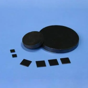
Single Crystal Cadmium Sulfide Wafer CdS Substrate
- Category: >>>
- Supplier: Xiamen Zopin New Material Limited
Share on (1601002343483):
Product Overview
Description
Product Description

Introduction
The semiconductor compound cadmium sulfide(CdS) has a photovoltaic effect and can be used to make a solar cell. Due to its special electrical, optical, semiconductor and optoelectronic properties, the CdS substrate has received extensive attention. The II - VI crystals are likely to be used for highlight shots in the near future. Their direct bandgap properties and wide range of transparency as well as a bandgap offer a wide range of possibilities for interesting equipment.
Specification
Specification
The main performance parameters | ||
Product Name: | CdS single crystal substrate | |
Growth method | PVT | |
Crystal Structure : | Hexagonal system | |
Lattice constant: | a=4.1367; c=6.7161 | |
Melting point: | 1287 ℃ | |
Density: | 4.821 g/cm3 | |
Heat capacity(J /g.k) | 0.3814 | |
Thermal expansion coefficient(10-6/K) | 4.6 // a 2.5 // c | |
Thermal Conductivity( W /m.k at 300K ) | 2.7 | |
Transparent wavelength( um) | 2.5 ~ 15 (>71%) | |
Refractive index | 1.708 (o) 1.723 (e) | |
Orientation | <0001> ±0.5º | |
Standard Size | 10x10x0.5mm, 5x5x0.5mm | |
Polishing | One side polished or Two side polished | |
Packing | class-100 clean bag, in class-1000 clean room | |

Company Profile


Cooperative Partner

Customers Feedback

Package & Transport

FAQ

Q1:What is the pore size on the foam and what is the PPI range?
A:100um<pore size<10mm, PPI range is 5ppi-500ppi.
Q2:Do you accept credit card payment?
A:We accept any payment method, credit card, bank transfer, Paypal, etc.
Q3:Can you customize the size and shape?
A:Yes, we accept customization, not only the size and shape, but also PPI or porosity and pore size.
Q4:Can I place one small order for first time to test the quality?
A:Small order are also welcomed.
Q5:Can I visit your factory?
A:Your are welcomed to visit our factory,and we offer free hotel and free car.
Home

We Recommend
New Arrivals
New products from manufacturers at wholesale prices


