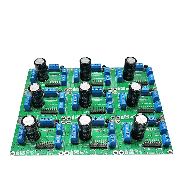
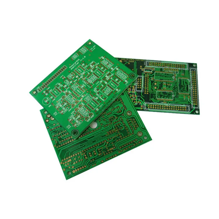
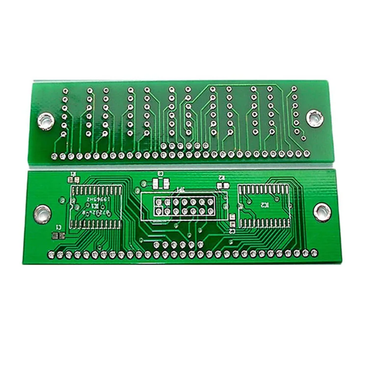
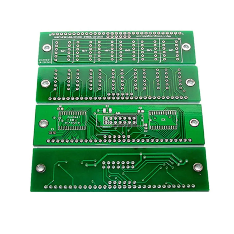
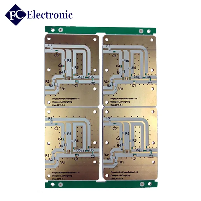
High quality PCB board for weighing scale
- Category: Multilayer PCB >>>
- Supplier: Shenzhen Xing Da Electric Technology Co. Ltd. [Guangdong China]Shenzhen
Share on (60116161981):
Product Overview
Description
Welcome to XingDa Electric Technology Co.,Ltd
We are professional manufacturer in various PCB and PCBA with many years experience,We can provide a reasonable price with high quality products.
1. PCB and PCBA product with below advantages:
1. PCB layout, PCB professional design
2: Make high difficulty PCB(1 to 38 layers)
3: Provide all Electronic components
4: PCB assembly
5: Write programs for clients
6: PCBA/finished product Test. etc.
2.Quote requirement
1).OEM&ODM are welcome!
2).Gerber files and specification;
3).FR4/CEM-3 PCB samples for us;
3.Why choice us?
Quality
OurRohs standards insure quality assemblies from start to finish. Whether it's a simple custom product or a complex turnkey production run, XingDa will adhere to the highest quality standards.
Capable
XingDa offers the latest in assembly capabilities and qualifications insuring that quality is built into every product we produce.
Experience
When it comes to your build you want a partner you can depend on. Our management team has over 10years of combined industry knowledge. Our engineering team has over 8 years experience.
Protecting your interests
Protecting your Intellectual Property is job one! Our staff colleague of trained professionals are all working under a strict confidentiality contract and treat your important documentation as they would their own.
Flexibility
XingDa pride ourselves on our ability to custom tailor programs around our customers' needs. We take time to listen to your unique business needs and then set out to surpass them.
4. PCB Manufcture Capacity
|
Item |
Specification |
|
Numbr of Layer |
1-38Layers |
|
Material |
FR-4,FR2.Taconic,Rogers, CEM-1 CEM-3,ceramic , crockery Metal-backed Laminate |
|
Finish Board Thickness |
0.2mm-6.00 mm(8mil-126mil) |
|
Minimun Core Thickness |
0.075mm(3mil) |
|
Copper Thickness |
1/2 oz min;12 oz max |
|
Min.Trace Width & Line Spacing |
0.075mm/0.1mm(3mil/4mil) |
|
Min.Hole Diameter for CNC Driling |
0.1mm(4mil) |
|
Min.Hole Diameter for punching |
0.9mm(35mil) |
|
Biggest panel size |
610mm*508mm |
|
Hole Positon |
+/-0.075mm(3mil) CNC Driling |
|
Conductor Width(W) |
0.05mm(2mil)or;+/-20% of original artwork |
|
Hole Diameter(H) |
PTH L:+/-0.075mm(3mil);Non-PTH L:+/-0.05mm(2mil) |
|
Outline Tolerance |
0.125mm(5mil) CNC Routing;+/-0.15mm(6mil) by Punching |
|
Warp & Twist |
0.70% |
|
Insulation Resistance |
10Kohm-20Mohm |
|
Conductivity |
<50ohm |
|
Test Voltage |
10-300V |
|
Panel Size |
110×100mm(min);660×600mm(max) |
|
Layer-layer misregistration |
4 layers:0.15mm(6mil)max;6 layers:0.25mm(10mil)max |
|
Min.spacing between hole edge to circuity pqttern of an inner layer |
0.25mm(10mil) |
|
Min.spacing between board oulineto circuitry pattern of an inner layer |
0.25mm(10mil) |
|
Board thickness tolerance |
4 layers:+/-0.13mm(5mil);6 layers:+/-0.15mm(6mil) |
|
Impedance Control |
+/-10% |
|
Different Impendance |
+-/10% |
5.The view of XingDa
a.PCB factory

b.PCBA factory

c.Test corner

We Recommend


New Arrivals
New products from manufacturers at wholesale prices


