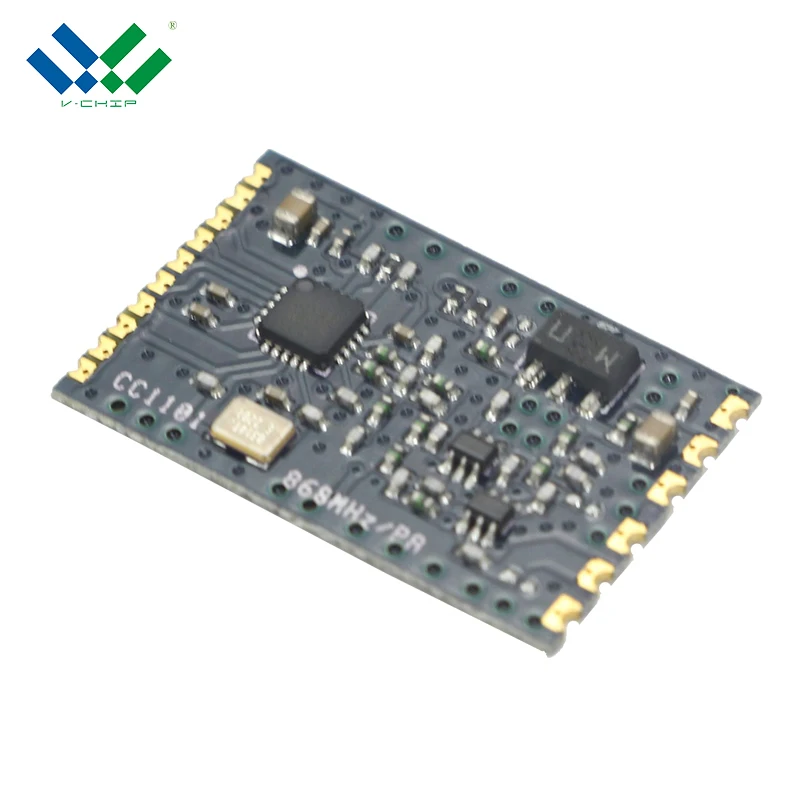
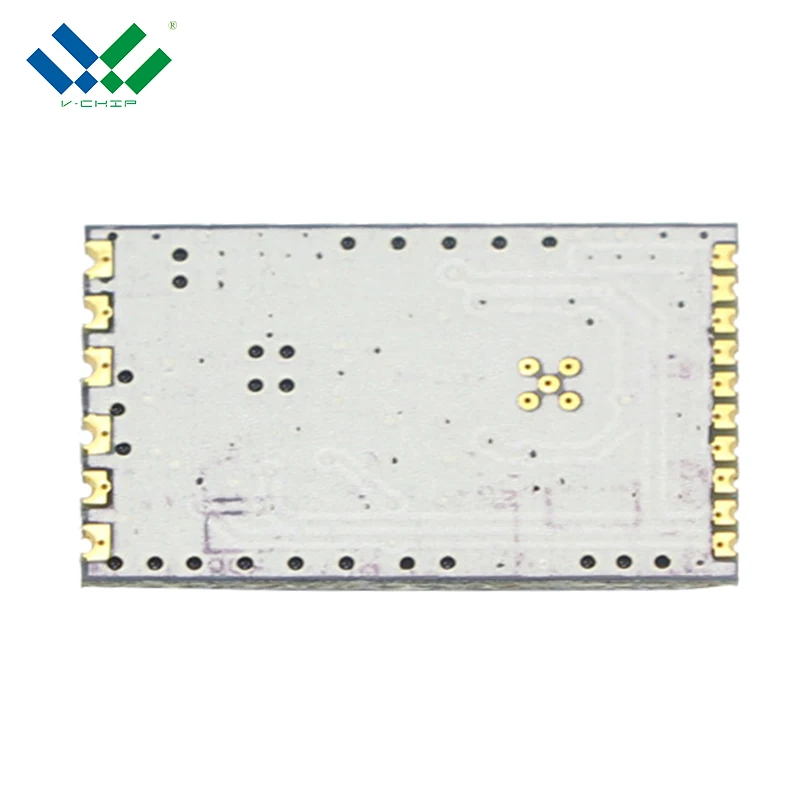
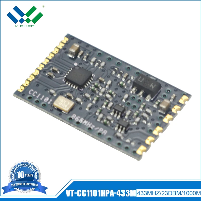
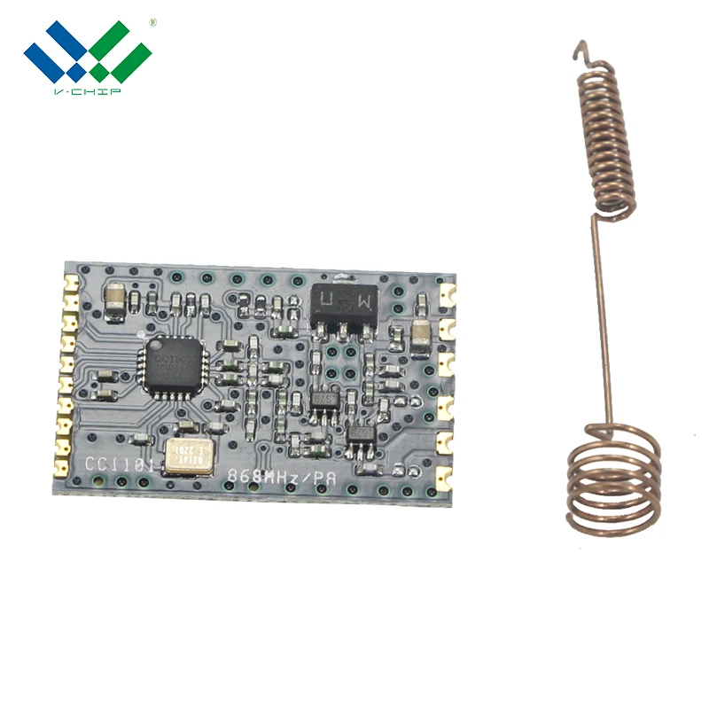
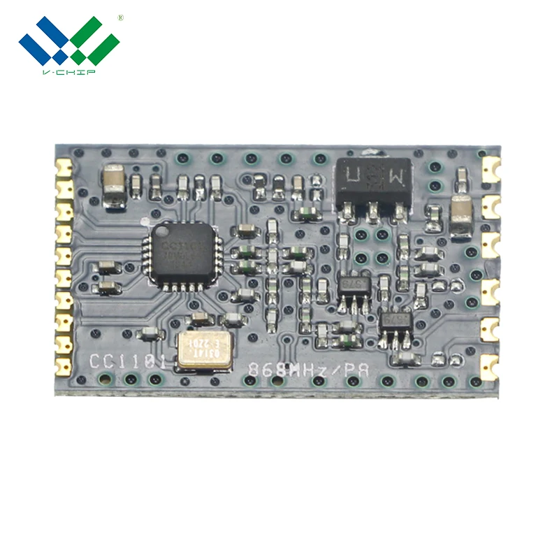
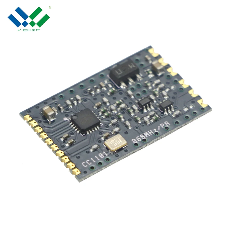
High Power 1KM 20dbm CC1101 PA Digital FSK TX RX 433MHz 868MHz Module for Remote Control
VT-CC1101HPA-433/868/915M is based on RF Transceiver CC1101 of TI Chipcon,it’s a small size and ultra low power UHF wireless module.CC1101 is a low cost true single chip UHF transmitter designed for very low power wireless applications. The circuit is mainly intended for the ISM (Industrial, Scientific and Medical) and SRD (Short Range Device) frequency bands at 315, 433, 868 and 915 MHz, The MAX RF output power can be set as high as +10dBm, with data rate as high as 500Kbps. The module integrated many RF functions and PA to make the maximum output power up to +30dBm. Customer can use it conveniently and reducing your development time.
Detail Parameters
Parameter
Type
Condition/Note
Operating supply voltage
DC 3.0~3.6V
Central frequency
433MHz
Can be programmable to other frequency in bands 387~464MHz
Frequency accuracy
±10KHz
Modulation format
GFSK/2-FSK/ASK/OOK/MSK
Programmable
Transmit power
20dBm
Programmable
TX current consumption
<250mA
Po=30dBm
Receiver sensitivity
20dBm
2.4Kbps
RX current consumption
<22mA
2.4Kbps
Sleep State current consumption
<2uA
Refer to IC operation states
Data rate
1.2~500Kbps
Programmable
Spurious emissions and harmonics
< -30dBm
TX power +10dBm.
Communication distance
>1200m
Use VT-CC1101-433M as a receiver, 2-FSK modulation, 1.2kBaud data rata, +10dBm output power.
Antenna impedance
50ohm
Operating temperature
-20~+75 °C
Storage temperature range
-50~+125°C
Dimension
26.0 mm×17.0 mm×2.4mm
See more in PCB description
Test operating conditions:Ta=25°C,VCC=3.3V if nothing else stated.
Note:
1. The module transmission data rate will affect Transmission distance ,the higher the data rate , the closer the distance, and the lower the receiving sensitivity.
2. The supply voltage to the module will affect TX power, in the operating supply voltage range, the lower the voltage, the lower the TX power.
3. The module central frequency will change as the operating temperature change, use it under suggest temperature, the module can work well.
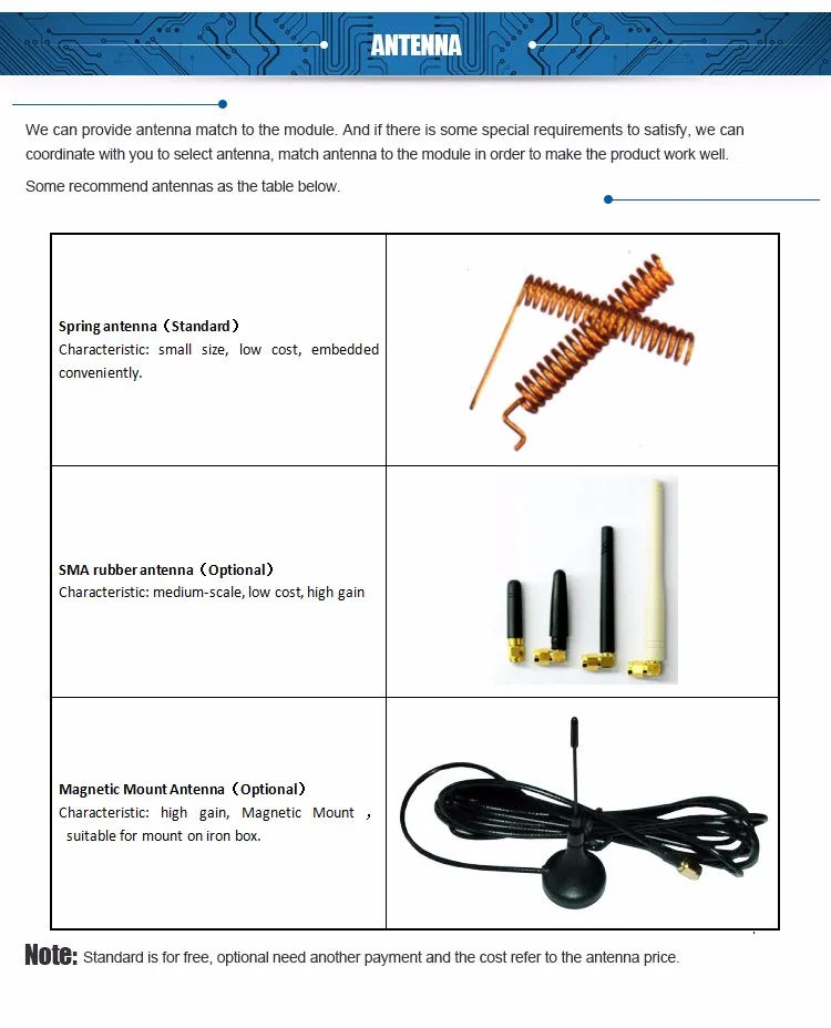
4. The antenna will strongly affect the communication distance, please select matched antenna and connect it correctly.
5. The module mount will affect the communication distance.
Features
Related Product
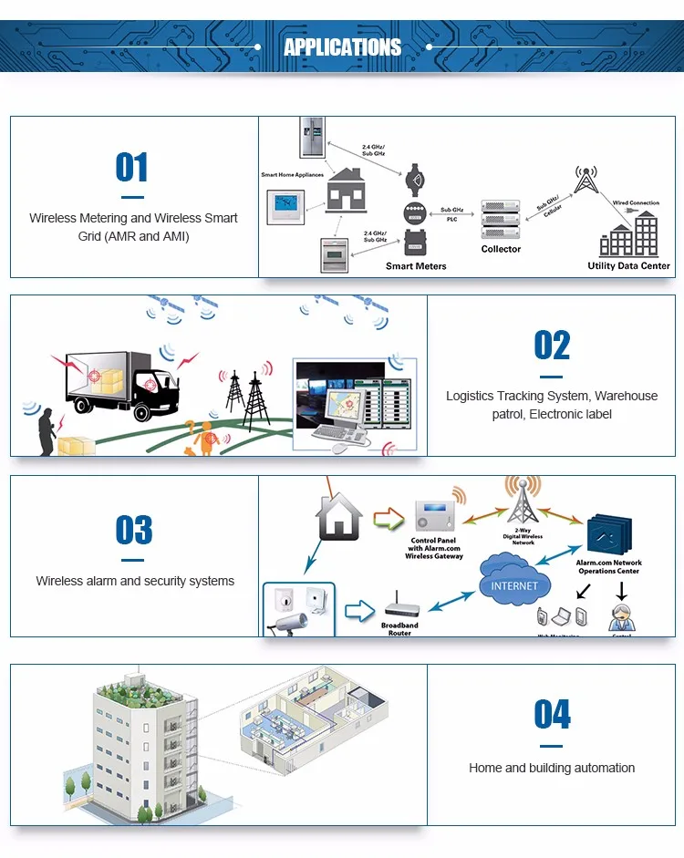
Applications
Pin name
Pin type
Description
3.3V
Power(Analog)
1.8 V - 3.6 V analog power supply connection.
GND
Ground
Connect to the system ground.
SI
Digital Input
Serial configuration interface, data input.
SCLK
Digital Input
Serial configuration interface, clock input.
SO
Digital Output
Serial configuration interface, data output.
Optional general output pin when CSN is high.
GDO2
Digital I/O
Programmable Clock output, down-divided from XOSC
GDO0
Digital I/O
Programmable Clock output, down-divided from XOSC.
CSN
Digital Input
Serial configuration interface, chip select, active low.
RE
Digital Input
RX state: RE=0(Low), TE=1(High)
TX state: RE=1(High), TE=0(Low)
TE
Digital Input
VDD
Power(Analog)
DC voltage from 3.0~9V input
ANT
RF I/O
RF output signal from PA, connect to the Antenna.
Note:
1. The module power supply voltage range is DC 3.0~3.6V, the PA supply voltage is DC 3.0~9.0V,above DC 3.6V, the module will damage. It is recommended work at DC 3.3 V, the PA supply voltage consider the application condition.
2. The module interface use half circle pad to soldering on the system PCB board, the GND must soldering to the system digital GND reliably.
3. The antenna must the get to the module’s ANT pin as close as possible.
4. The MCU which don’t have integrated SPI interface can also control the module, use the normal I/O port to work like SPI timing to read and write. The SPI data rate is below 10MHz.
5. The interface can connect directly to the MCU which use 3.3V power supply, there is no need serial resistor. If the I/O is open-drain, the pull-up resistor will be added. When connect to the MCU which use 5V power supply, the MCU’s I/O output current beyond 10 mA, a 2~5k ohm resistor will be series to divide the voltage, or it will damage the module.
6. The module’s pin GDO0 and GDO2 are general digital I/O ports, they can be programmable to produce trigger signal or clock output.
7. The PA control voltage have an effect on the communicate distance and power consumption. In transmit mode, set TE=0 and RE=1; in receive or sleep mode, set TE=1 and RE=0.
8. In the multiple channel application, the channel spacing is recommended to set as 1MHz, or there will be a same frequency interference.
9. The module TX power and current consumption reference to the PA supply voltage list in the table below:
Power amplifier voltage(VDD)
PO (dBm)
Consumption current(mA)
3.0V
21.63
97
3.6V
22.98
111
4.5V
24.61
132
5.0V
25.34
142
6.0V
26.52
161
7.0V
27.33
176
7.5V
28.11
185
9.0V
28.71
204
Company Information
Packaging & Shipping
FAQ
Description
Reason and Solution
Can’t communication
1.The power supply connect not well, check the module VCC whether it is out of maximum rating.
2.The signal line connect not well, check the module SPI interface.
3.The settings of the transmitter module and receiver module are not the same. Check these modules’ register configuration.
4.Signal block. If the transmitter work with a high TX power, and the receiver was put at a short distance(<0.5m), maybe there is a signal block to make no communication.
Communication distance is too short
1.The application environment is too bad or the antenna is shield. Put the antenna to a better place outside or higher throw a coaxial line , replace it with a higher gain antenna.
2.The work space contains a same frequency interference source, or a strong magnetic field interference,power source disturbance. Try to change the carrier frequency or get far away from the source of the disturbance.
3.The power supply is not strong. Check the voltage and the current whether it is enough.
High data error
1.The power supply ripple is too big, Change the power supply.
2.Check the module register configuration, it is recommended to set as the CC1120-datasheet.
3.There is a carrier frequency interference, change the channel.
4.The antenna unmatched to the module RF interface, change another matched antenna.