
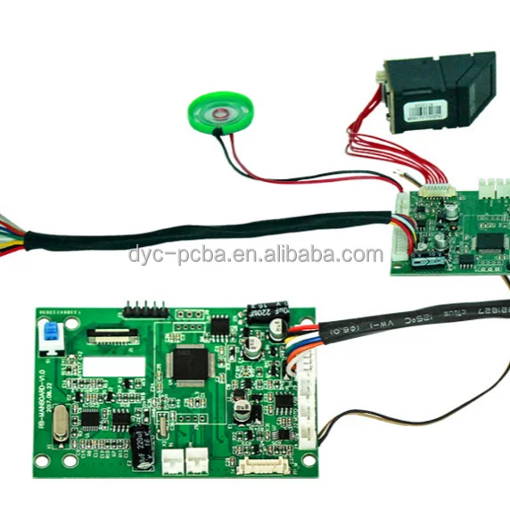
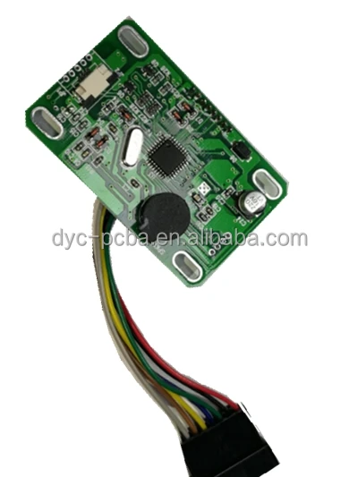
fingerprint unlocking coded lock RFID LOCK PCB schematic design and layput services
- Category: Double-Sided PCB >>>
- Supplier: Shenzhen Dyc Electronic Technology Co. Ltd.
Share on (60733351533):
Product Overview
Description
Company Information

DYC Electronic is a professional PCB&PCBA manufacturer who has dedicated to printed circuit board designing, producing and PCB assembly service with more than 10 years experience, our company was founded in September 2007;the factory is located at Shenzhn, China. After 10 years developing, we are a top site PCB&PCBA manufacturer now in China with more than 300 employees.
fingerprint unlocking coded lock RFID LOCK PCB schematic design and layput services
Our services:
1. PCB design ,PCB clone and copy ,ODM service.
2. Schematic design and Layout.
3. Fast PCB&PCBA prototype and Mass Production.
4. Electronic Components Sourcing Services.
5. PCB Assembly Services:SMT,DIP&THT,BGA repair and reballing.
6. ICT, Constant Temperature Burn-in and Function Test.
7. Stencil,Cables and Enclosure building.
8. Standard Packing and On time Delivery.
Our advantage:
1. 24 hours online one-stop service
2. Quick response and delivery.
3. Strict quality management.
4. Professional engineering and technical team
5. Electronic components from the original.
6. Long - term cooperative shipping company.
7. Free samples.
8. Excellent after-sales service.
Our PCB design Capability
1. Design Layers: Single and above.
2. The highest signal frequency: Microwave 24GHz, differential 12G signal.
3. Maximum single load current: 100A.
4. Minimum BGA PIN Pitch: 0.4mm.
5. Maximum PIN number: 47698.
PCB &PCBA Capability
Our PCB Capability
Layer:1~30 layers
Materials: FR-4, CEM-3, Teflon, Aluminum, Rogers, High Tg
Surface finished:Lead Free HASL,Immersion Gold/Tin/Silver, OSP, Gold Finger Plating, Selective Immersion Gold,Gold Plating.


Our PCBA Capability

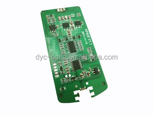
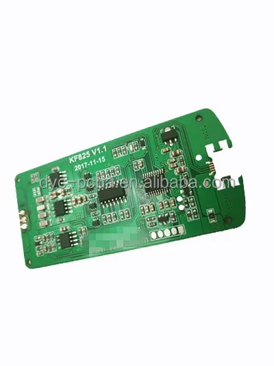
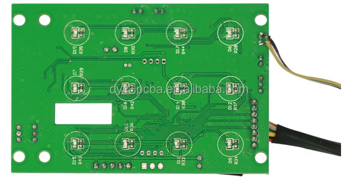
Product Description


![0)79[A[}8P)$C%(X8J`CN]N](http://sc02.alicdn.com/kf/HTB1l4Nwl_nI8KJjSszg7638ApXa9/221266742/HTB1l4Nwl_nI8KJjSszg7638ApXa9.png)

Our payment :

Our shipment:

Packaging Details:
Inner packing: Vacuum and Anti-static bubble bag.
Outer packing: High standard cartons box.
Delivery Details: Sample5-7 days; Mass:15-25days
Shipping:
We haveour own forwarder support you best shipment way with the competitive price,save your time and money.
Please contact us if any question:

FAQ
Q1: How do you make sure the quality of the PCBs?
A1: Our PCBs are all 100% test including Flying Probe Test, E-test or AOI.
Q2: What is the lead time?
A2: Sample needs 2-4 working days, mass production needs 7-10 working days. It depends on the files and quantity.
Q3: Can I get the best price?
A3: Yes. To help customers control cost is what we are always trying to do. Our engineers will provide the best design to save the cost of PCB material.
Q4: What files should we Provide for a customized order?
Q4: If only need PCBs, the Gerber files are needed; If need PCBA, both Gerber files and BOM are needed;If need PCB design,all requirement details are needed.
Q5:Can I get a free sample?
A5:Yes, Welcome to experience our service and quality.you need make the payment at first,and we will return the sample cost when your next bulk order.
We Recommend


New Arrivals
New products from manufacturers at wholesale prices


