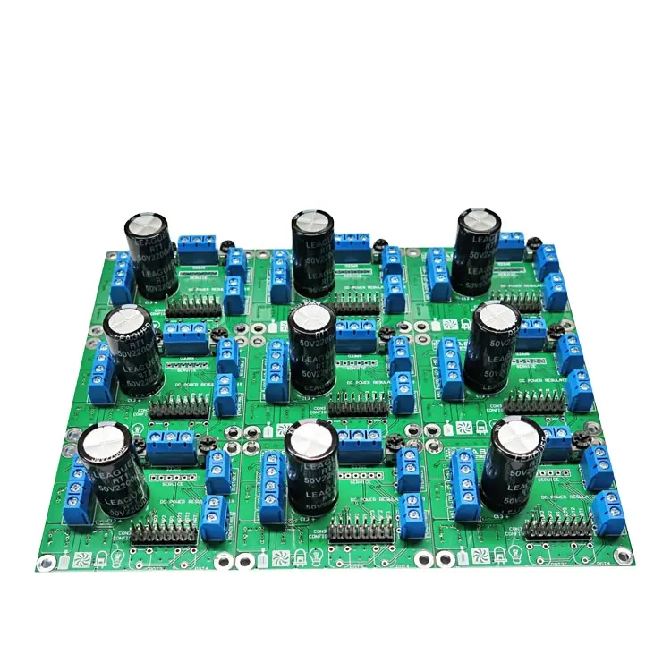
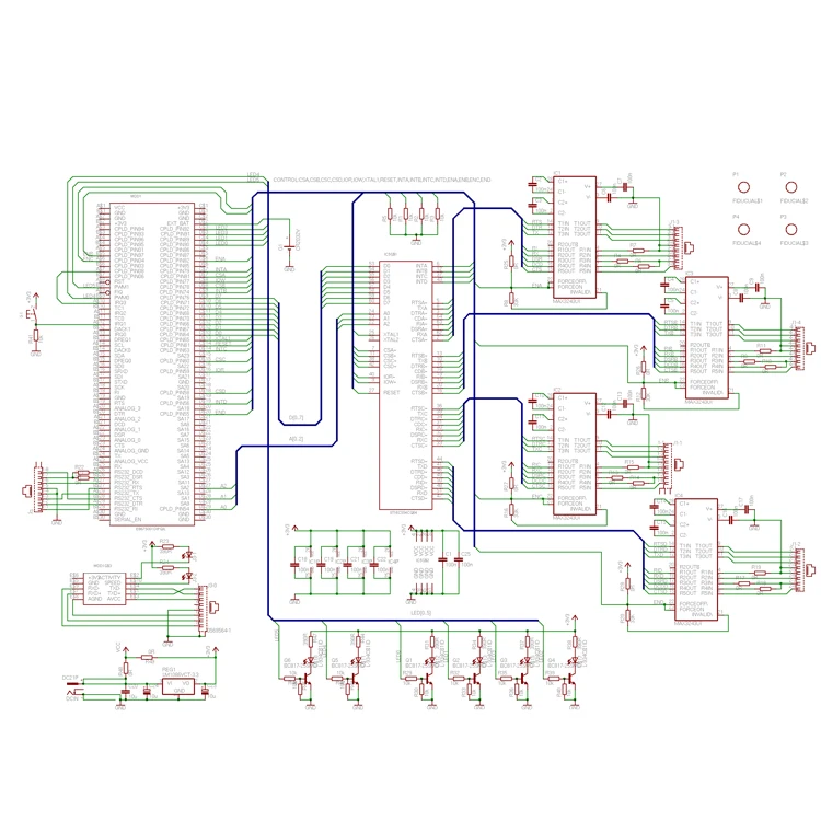
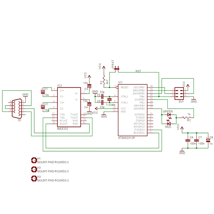
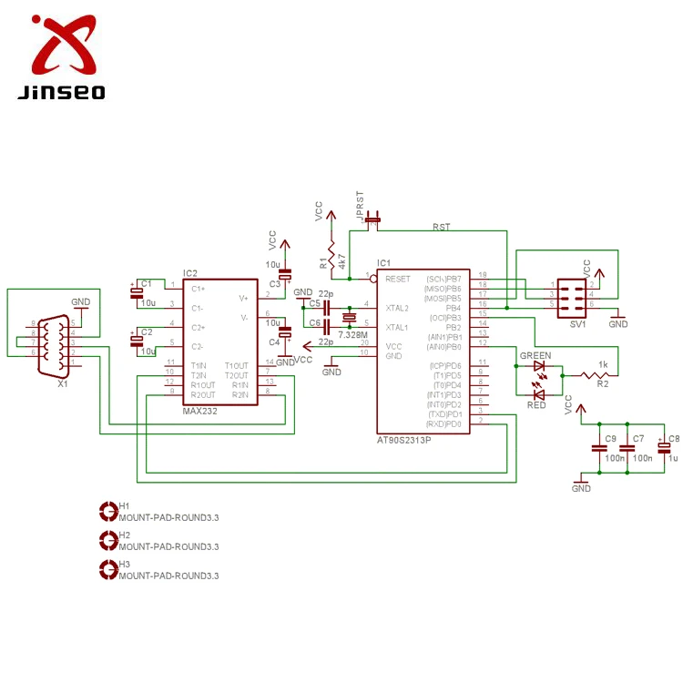
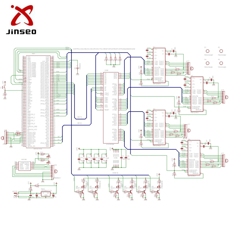
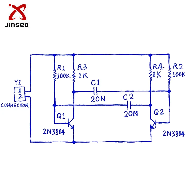
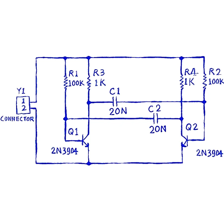
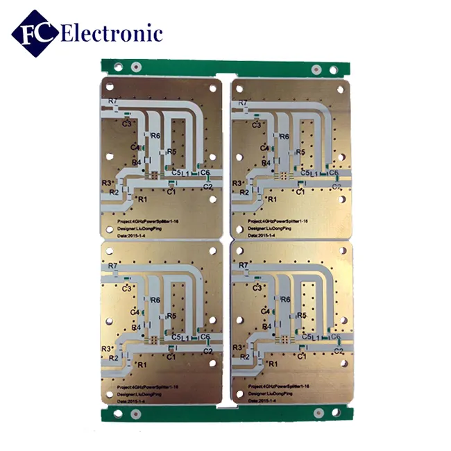
Fr4 led pcb schematic diagram circuit board pcb design manufacturers
- Category: Multilayer PCB >>>
- Supplier: Dalian Jinseo Electronic Technology Co. Ltd.
Share on (60754645567):
Product Overview
Description

Fr4 led pcb schematic diagram circuit board pcb design manufacturers

Specs for Flex pcb:
| PRODUCT | STANDARD FLEX CIRCUITS | STANDARD RIGID-FLEX CIRCUITS | HIGH DENSITY INTERCONNECT (HDI) FLEX CIRCUITS | |||
| STANDARD PANEL SIZE | 250mm x 450 mm | 100mm x 100mm | 250mm x 450mm | |||
| LINE WIDTH AND SPACING | .0015" (0.04mm) | .003" (0.07mm) | .003" (0.07mm) | |||
| COPPER THICKNESS | 1/3 oz. and higher | 1/4 to 1/2 oz. | 1/2 oz. and higher | |||
| LAYER COUNT | 10 | Up to 4 | Up to 18 | |||
| VIA/DRILL SIZE | ||||||
| MINIMUM DRILL (MECHANICAL) HOLE DIAMETER | .006" (0.15 mm) | .006" (0.15 mm) | .008" (0.2 mm) | |||
| MINIMUM VIA(LASER) SIZE | 4 mil (0.10 mm) | 1 mil (0.025 mm) | 6 mil (0.15 mm) | |||
| MINIMUM MICRO VIA (LASER) SIZE | 3 mil (0.07 mm) | 1 mil (0.025 mm) | 3 mil (0.07 mm) | |||
| STIFFENER MATERIAL | Polyimide /FR4 / Metal | Polyimide /FR4 / Metal | Polyimide / FR4 | |||
| SHIELDING MATERIAL | Copper / Silver Ink / Tatsuta / Carbon | Copper / Silver Ink / Tatsuta / Carbon | Copper / Silver Ink / Tatsuta / Carbon | |||
| TOOLING TOLERANCE | 2 mil (0.05 mm) | 1 mil (0.025 mm) | 2 mil (0.05 mm) | |||
| ZIF TOLERANCE | 2 mil (0.05 mm) | 1 mil (0.025 mm) | 2 mil (0.05 mm) | |||
| SOLDER MASK | ||||||
| SOLDER MASK BRIDGE BETEEN DAM | 4 mil (0.10 mm) | 4 mil (0.11 mm) | 4 mil (0.10 mm) | |||
SOLDER MASK REGISTRATION | 4 mil (0.11 mm) | 4 mil (0.11 mm) | 4 mil (0.10 mm) | |||
| COVERLAY | ||||||
| COVERLAY REGISTRATION | 4 mil (0.10 mm) | 5 mil (0.13 mm) | 8 mil (0.20 mm) | |||
| PIC REGISTRATION | 7 mil (0.18 mm) | 4 mil (0.11 mm) | 7 mil (0.18 mm) | |||
| SOLDER MASK REGISTRATION TOLERANCE | 4 mil (0.10 mm) | 4 mil (0.11 mm) | 5 mil (0.13 mm) | |||
| STIFFENER | ||||||
| PI STIFFENER | ||||||
STIFFENER REGISTRATION | 8 mil (0.20 mm) | 10 mil (0.25 mm) | 10 mil (0.25 mm) | |||
THICKNESS TOLERANCE | 10% | 10% | 10% | |||
| FR4 STIFFENER | ||||||
STIFFENER REGISTRATION | 8 mil (0.20 mm) | 10 mil (0.25 mm) | Layer to Layer | |||
THICKNESS TOLERANCE | 10% | 10% | 5 mil (0.13 mm) | |||
| LEGEND | ||||||
| MINIMUM HEIGHT | 35 mil (0.89 mm) | 25 mil (0.64 mm) | 35 mil (0.89 mm) | |||
| MINIMUM WIDTH | 5 mil (0.15 mm) | 5 mil (0.15 mm) | 5 mil (0.15 mm) | |||
| MINIMUM SPACE | 5 mil (0.15 mm) | 5 mil (0.15 mm) | 5 mil (0.15 mm) | |||
| REGISTRATION | +/- 5 mil (0.13 mm) | +/- 5 mil (0.13 mm) | +/- 5 mil (0.13 mm) | |||
| IMPEDANCE | +/- 10% | +/- 10% | +/- 10% | |||
| SRD (STEEL RULE DIE) | ||||||
| OUTLINE TOLERANCE | 5 mil (0.13 mm) | 2 mil (0.051 mm) | 5 mil (0.13 mm) | |||
| MINIMUM RADIUS | 5 mil (0.13 mm) | 4 mil (0.11 mm) | 5 mil (0.13 mm) | |||
| INSIDE RADIUS | 20 mil (0.51 mm) | 10 mil (0.25 mm) | 31 mil (0.79 mm) | |||
| PUNCH MINIMUM HOLE SIZE | 20 mil (0.5 mm) | 31.5 mil (0.80 mm) | N/A | |||
| TOLERANCE OF PUNCH HOLE SIZE | +/- 2 mil (0.051 mm) | +/- 1 mil (0.025 mm) | N/A | |||
| SLOT WIDTH | 20 mil (0.51 mm) | 15 mil (0.38 mm) | 31 mil (0.79 mm) | |||
| TOLERANCE OF HOLE TO OUTLINE | +/- 3 mil (0.07 mm) | +/- 2 mil (0.051 mm) | +/- 4 mil (0.11 mm) | |||
TOLERANCE OF HOLE EDGE TO OUTLINE | +/- 4 mil (0.11 mm) | +/- 3 mil (0.07 mm) | +/- 5 mil (0.13 mm) | |||
| MINIMUM OF TRACE TO OUTLINE | 4 mil (0.10 mm) | 5 mil (0.13 mm) | 10 mil (0.25 mm) | |||


To ensure an accurate quote, be sure to include the following information for your project:
Your custom quote will be delivered in just 2-24 hours, depending on the design complexity. |


How do we keep our prices low?We have relationships with a large number of board manufacturers and can find the best source of PCBs to consistently save your cost, meet your development schedule, fulfill your prototyping or mass production needs.What is Test NRE?The Test NRE is a one-time "non recurring expense" for electrical test. This charge is optional but when paid, all circuit boards will be tested each and every time that part number and revision is ordered without additional charge.When do you pay a tooling NRE fee for my printed circuit board?You will only pay a Tooling charge if you go directly to Production (Custom Spec) without having ordered a Proto (Standard Spec) as a first step. We do not charge Tooling for Protos (Standard Spec) and neither do we charge Tooling if the proto (Standard Spec) is reordered for Production (Standard Spec).If you only have a minor change in my design, do we charge Tooling NRE?When you make any change to your printed circuit board, we assign it completely new tooling. This helps prevent old artwork or cnc programming from being used. Even a minor change will require the same process as new files, so a tooling charge may apply. Please contact your salesperson for details.Are your "Prototype" PCBs processed differently from your Custom Spec PCBs?No. Our Standard Spec ("prototype") use the same premier manufacturing processes as our production(Custom Spec) circuit boards.To what acceptability standards do we build?IPC A600 Class 2 through IPC 6012 Class 3AWhere should you send your files to get a printed circuit board quote or place an order?You can simply send us an inquiry via Alibaba site. Very soon our sales person will contact you for your inquiry/files. Or you can send your inquiry/files to “Marketing at jinseo.com.cn”How fast can you get a quote after submitting an inquiry?We will on receipt of your file evaluate in 6 hours for standard spec PCB. But if PCB special, evaluation will be longer. Please note that the following detail will speed up evaluation:Material: Board thickness: Copper thickness: Surface finish: Solder mask color: Silkscreen color:
What is our Warranty on PCBs?
90 DAY LIMITED WARRANTY We warrant our bare boards against defects in materials and workmanship under normal use for a period of 90 days from date of shipment ("Warranty Period"). If a defect arises and a valid claim is received within the warranty period, We will, at our option, for any bare boards that are returned and confirmed by us to be non-conforming to the order specifications and/or the applicable quality and acceptability standards, either (I) replace the bare board at no charge or (II) issue a credit equal to the original purchase price of the bare board. |
We Recommend


New Arrivals
New products from manufacturers at wholesale prices


