

- Home
- Categories
- GPS Disciplined Oscillator with 2 Clock/RF output channels

GPS Disciplined Oscillator with 2 Clock/RF output channels
- Category: >>>
- Supplier: Shenzhen Chen-N Technology Co. Limited
Share on (60778299749):
Product Overview
Description
Product Description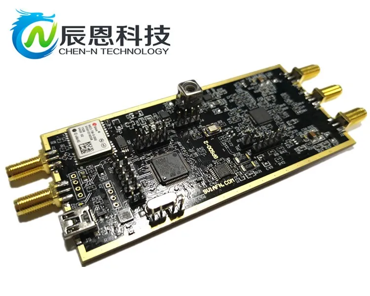

Get 2 RF/clock output channels independently set on any frequency from 100 HZ - 1028 MHZ (integer or fractional) locked to the GPS time-signal's accuracy and stability


The idea was to use a GPS receiver's time pulse output as a reference, for frequency stability and frequency accuracy, without needing a calibration or periodic adjustment. Then, to use this signal together with another oscillator's signal (of the on-board 50 MHZ TCXO's or any external TCXO or OCXO...) to take advantage of its low phase-noise and numerically manipulate with a highly-complex digital PLL chip like the Silicon Labs Si5342A-D, to phase lock any output frequency from KHZ to GHZ having the qualities of the stability and accuracy of the GPS signal and the low-phase noise of the TCXO's used, well or close enough. It may not be possible as simple and as general as written above, but it worths the try!
This project was made at first to accompany the SV1AFN's HF Up-Converter with the purpose to replace its 200 MHZ internal oscillator used as a Local Oscillator for the mixing circuit to obtain higher accuracy and stability but with the best phase noise, as needed for best HF receiving performance. Having a 2nd channel available, a clean 10 MHZ signal to synch test equipment around the lab using an external distribution amplifier is always welcome. Since then, many new applications found and the latest design has now an ARM-type micro-controller, the STM32L152RET6 which has a USB interface.
The user can download Silicon Labs "Clock Builder Pro" software, arrange all internal functions and produce a register file for the Si5342A-D chip. Next, using a software interface written in Python load this register file, send it to the micro-controller for configuring the Si5342A-D. Or, even store it in E2PROM for later use without a USB interface needed (for set and forget applications like an external LO for radios, converters, clock for ADCs, DACs etc).
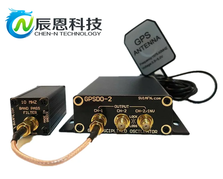
By using a UART interface the MCU talks to the GPS receiver to set its time signal output for 10.000.000 HZ at 50% duty cycle instead of 1PPS. This is the "0 ppm reference" signal for the Si5342A-D. The GPS receiver produces the signal when it finds satellites or stops producing it when the satellites signal is lost. This signal is noisy and cannot be used at its own but it's frequency is very accurate and stable. As for an initial clean-up, it passes through a series tuned network and then it is applied to the Si5342A-D clock input. If for any reason, the user needs to change the 10 MHZ GPS output frequency to any other value, then the tuned network should be bypassed, by placing any large capacitance on the C52 footprint, which is not populated by default.
The TXCO should be a 48-52 MHZ type and the PCB has two fooprints, U5 and U5ALT, with U5ALT populated with a TAITIEN TYKTDLSANF-50.000000, a +/- 2 ppm 50 MHZ 1.8V clipped sine-wave TCXO. A better but much more expensive TCXO can be placed on U5, a CONNOR WINFIELD D75J-050.0M, a less than +/- 1 ppm 50 MHZ 3.3V TCXO. If the 3.3V TCXO is used, the PCB has components for its output power reduction so to keep Si5342A-D's input safe from overdriving. Both TCXOs have good phase noise figures (like better than -120 dBc/Hz at 1 KHZ spacing). Any external TCXO or OCXO can be connected to pin 5 of the U5 PCB footprint if it is 3.3V or to pin 3 of U5ALT if it is a 1.8V type.
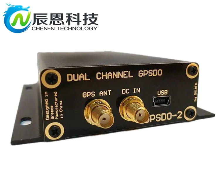
The board needs 5V DC at around 350 mA, the exact amount for the current consumption depends on the configuration of the two output interface types (LVDS, LVPECL, LVCMOS, CML, or HCSL), different termination loading and voltage levels.
If the GPS receiver looses fix the internal oscillator can be configured to produce the same or different frequency, of course with much less accuracy and stability because it will now be relied upon its internal oscillator. But an interesting feature of the Si5342 chip can be used and this is its "holdover mode": When the GPS receiver looses fix and configured not to output anything, i.e., stop producing the 10 MHZ signal, then the Si5342 by itself, detects the "loss-of-lock", LED LD1 lights, and switches to the "holdover" mode. The chip uses an averaged input clock frequency as its final holdover frequency to minimize the disturbance of the output clock phase and frequency when an input clock suddenly fails. The holdover circuit for the chip's DSPLL stores up to 120 seconds of historical frequency data while locked to a valid clock input. The final averaged holdover frequency value is calculated from a programmable window within the stored historical frequency data. Both the window size and the delay are programmable. The window size determines the amount of holdover frequency averaging. The delay value allows ignoring frequency data that may be corrupt just before the input clock failure. One may experiment and measure if this is the most accurate way to maintain the programmed output signals when the GPS receiver looses fix, or if it is better to configure the GPS receiver producing the 10 MHZ by its own internal reference oscillator when it losses the satellites signals. For this example, one can use the software interface to change the instructions sent over the UART to the GPS receiver. The interface allows modifying every single register's value if ever needed.
STABILITY & ACCURACYMeasurements: Have not been conducted yet, generally the output signals accuracy and stability it is assumed to follow that of the GPS with some added wander depending on the TCXO used. I understand this is a huge issue but metrology-purist friends may be able to help suggesting a clever method. For now, it is enough to say that the GPSDO will follow the GPS time signal accuracy and stability and if there is any difference it will be documented here at a later time.
PHASE NOISE measurements: The 10 MHZ LVCMOS (not the best selection for best phase noise performance) 3.3V level, 33 Ohm loading, single-ended output is measured with a Tektronix RSA-306 Real Time Spectrum Analyzer.
Attention: The phase noise is not the same on any programmable output frequency. We have not tested and measured phase noise on every frequency but generally it gets worsen as the frequency increases. A lot of parameters which can be changed in the Clock Builder Pro software deteriorates or improves phase noise in every instance. Choosing fractional or integer is less significant than originaly thought, adjusting target loop bandwidth is very important. One should experiment with different values to optimize phase noise on any wanted output frequency
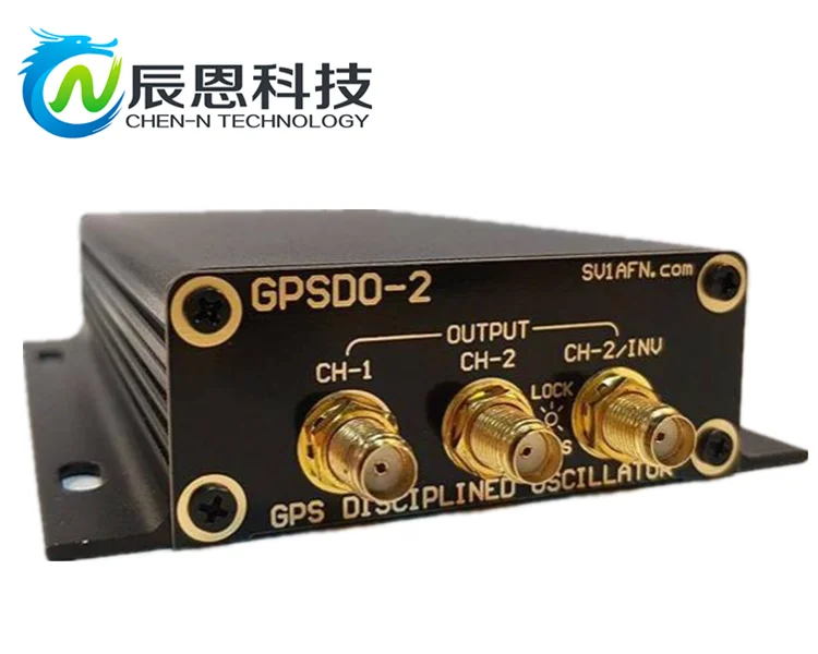
Output channels configuration:
The GPSDO-2 board has 3 SMA connectors for the 2 output channels, J2 is OUT0 single ended and J2 and J3 are the OUT1 and OUT1INV (balanced). Equal length traces are connecting the two SMA connectors J4 and J5 on the PCB and users can benefit of this feature to drive balanced ADC/DAC clock inputs or anything else. The Clock Builder Pro software allows controlling the phase polarity and instead of 180, 0 degrees can be chosen. If a user needs the complementary output of OUT0, which is not routed on the PCB, then a small coax can be very carefully soldered on pin 19 of U4.
Equipment


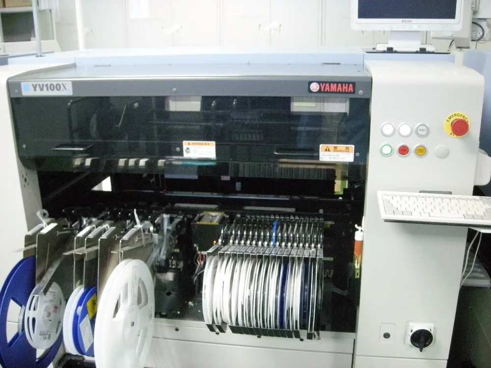


AOI
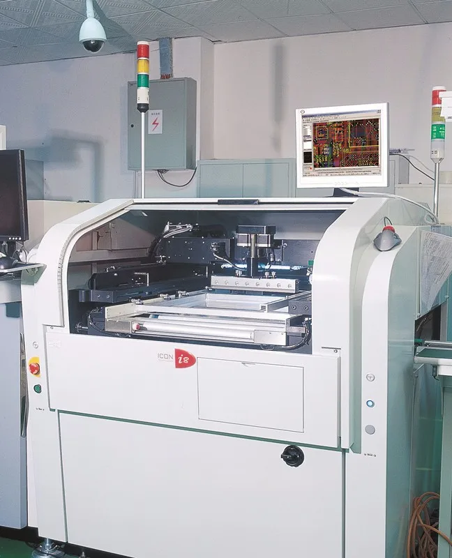
PRINTING
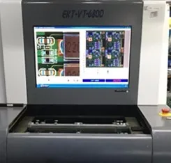
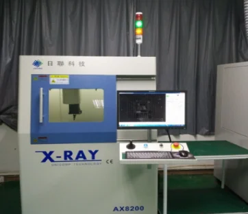
X-RAY
Our Company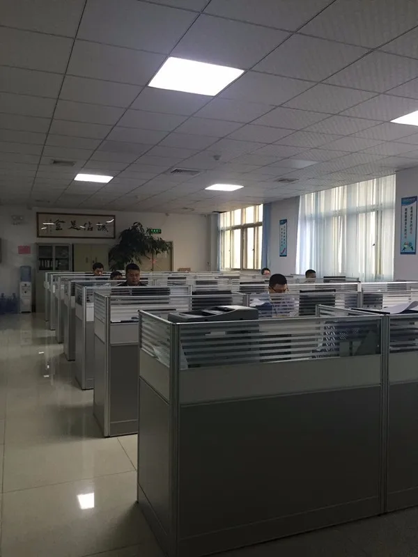


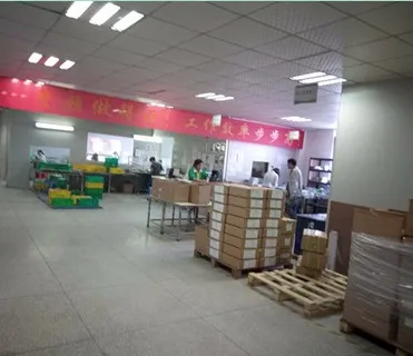
OFFICE
FACTORY
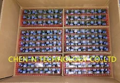
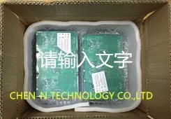
Delivery & Package


FAQ
Q: What do you need to quote ?
A:1,Gerber file
2,Quantity
3,Technical requirement
4,BOM list
Q: How long do you need to quote ?
A: 1,PCB &FPC: within 1 hour
2,PCBA : within 2 days
Q: Which method of payment you can accept?
A: T/T , Western Union,Paypal.
Q: How long can I get my order?
A:For samples,we'll finish the product and ship it within 7-10 working days. For bulk orders,usually 15-20 working days
CONTACT US
We Recommend

New Arrivals
New products from manufacturers at wholesale prices


