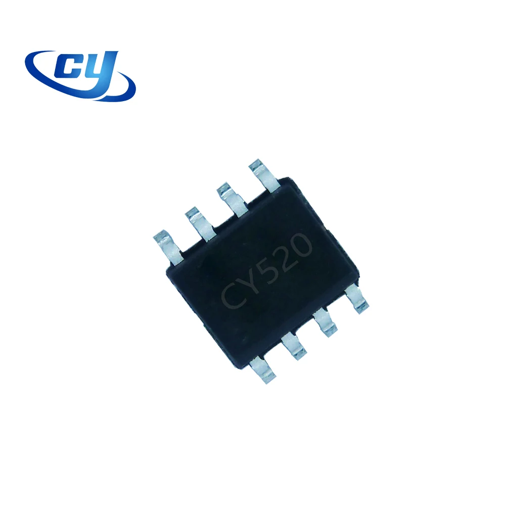
CY520 300M 450MHz 433mhz rf receiver ic
- Category: >>>
- Supplier: Shenzhen CY Wireless Technology Limited
Share on (60808245642):
Product Overview
Description
Product Description
The CY520 is a general purpose, 3.3-5V ASK Receiver that operates from 300M to 450MHz with typical sensitivity of -109dBm.
The CY520 functions as a super-heterodyne receiver for OOK and ASK modulation up to 10kbps. The down-conversion mixer also provides image rejection. All post-detection data filtering is provided on the CY520. Any one-of-four filter bandwidths may be selected externally by the user in binary steps, from 1.25 kHz to 10kHz. The user need only configure the device with a set of easily determined values, based upon data rate, code modulation format, and desired duty-cycle operation.
CY520 is the SOP8 package version.
Features
-109dBm sensitivity, 1kbps and BER 10E-02
Frequency from 300MHz to 450MHz
Supply Voltage form 3V to 5.5V
Image Rejection Mixer Data-rate up to 10kbps(fixed-mode)
Low power, 6.0mA, 3.3V @433.92MHz, 3.9mA, 3.3V @315MHz, continuous on data rates to 10kbps(Manchester Encoded)
No IF filter required
Excellent selectivity and noise rejection
Analog RSSI Output
Applications
Automotive Remote Keyless Entry (RKE)
Remote Controls
Remote fan and light control
Garage door and gate openers
Pin Configuration

| Pin Name | Pin Function |
| RO1 | Reference resonator input connection o Colpitts oscillator stage. May also be driven by external reference signal of 1.5V p-p amplitude maximum. |
| ANT | RF signal input from antenna. Internally AC coupled. It is recommended that a matching network with an inductor-to-RF ground is used to improve ESD protection. |
| VDD | Positive supply connection for all chip functions. |
| VSS | Negative supply connection for all chip functions except RF input. |
| RO2 | Reference resonator input connection to Colpitts oscillator stage, a 18pF capacitor is connected from this pin to GND during normal operation. |
| CAGC | AGC filter capacitor connection. CAGC capacitor, normally greater than 0.47μF, is connected from this pin to GND. |
| CTH | Demodulation threshold voltage integration capacitor connection. Tie an external capacitor across CTH pin and GND to set the setting time for the demodulation data slicing level. Values about 1nF are recommended and should be optimized for data rate and data profile. |
| DO | Demodulated data output |
Absolute Maximum Ratings (Note 1)
| Supply Voltage | +7V |
| Input Voltage | +7V |
| Junction Temperature | +150℃ |
| Storage Temperature Range | -65℃ to +150℃ |
| Lead Temperature(soldering, 10sec.) | +260℃ |
| Maximum Receiver Input Power | +10dBm |
| ESD Rating | Note 3 |
Operating Ratings (Note 2)
| RF Frequency Range | 300MHz to 450MHz |
| Supply Voltage | +3.0V to +5.5V |
| Input Voltage | 5.5V (Max.) |
| Maximum Input RF Power | -20dBm |
| Ambient Temperature | -30℃ to +85℃ |
Note 1. Exceeding the absolute maximum rating may damage the device.
Note 2. The device is not guaranteed to function outside of its operating rating.
Note 3. Device is ESD sensitive. Use appropriate ESD precautions. Exceeding the absolute maximum rating may damage the device.
Contact us for more details and datasheets

We Recommend
New Arrivals
New products from manufacturers at wholesale prices