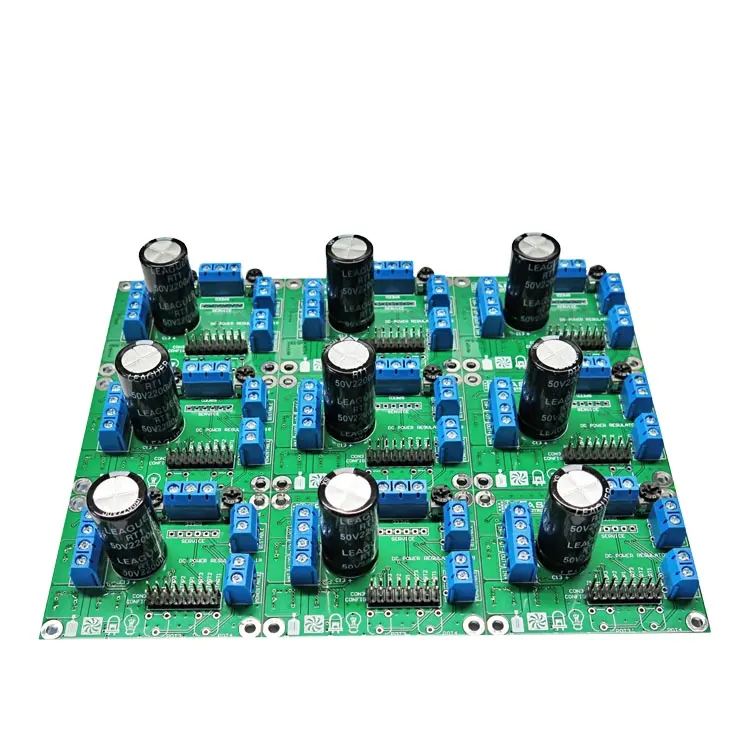
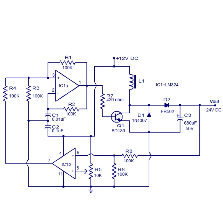

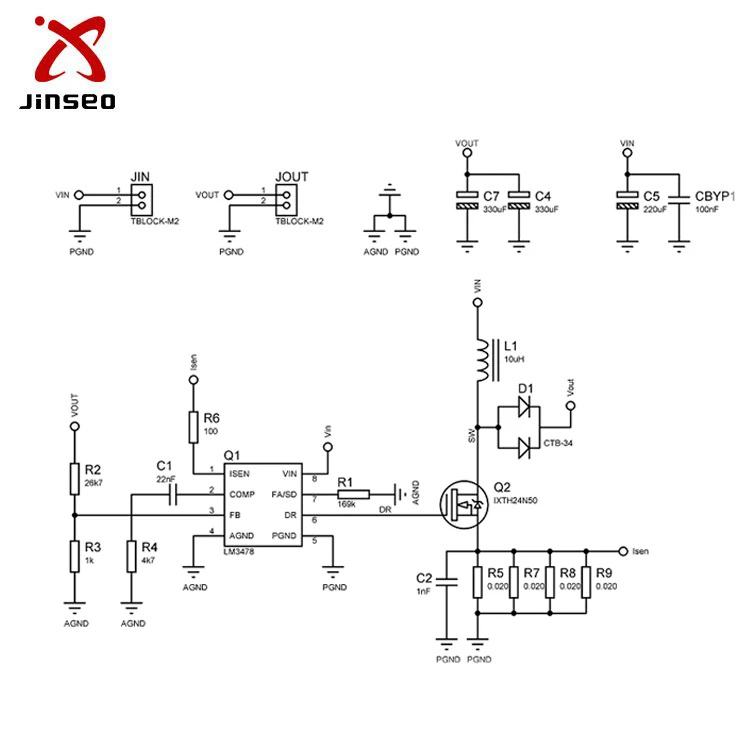
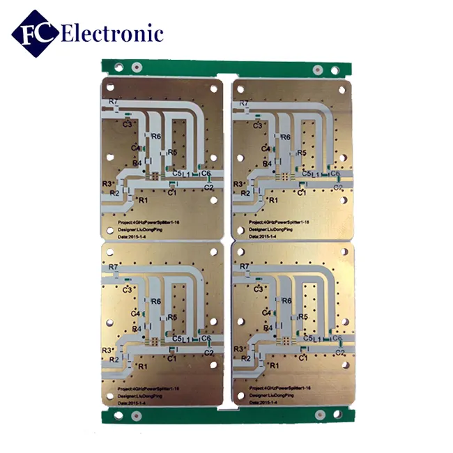
94v0 PCB electrical circuit diagram of welding machine Design
- Category: Multilayer PCB >>>
- Supplier: Dalian Jinseo Electronic Technology Co. Ltd. [Liaoning China]Dalian
Share on (60816114342):
Product Overview
Description


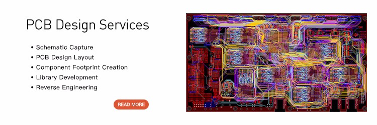


JINSEO PCB Design has the ability to complete your schematic capture and PCB layout in several different software packages including: • Cadence OrCAD/Allegro • Altium PCAD • Altium Designer |


• Acquire all information needed, reviewing and verifying the accuracy. • Schematic capture and net list generation (if not done yet). • Create part library for the project. • PCB component placement. • Submit intermediate placement to engineer for reviewing. This is usually a discussion- modification process until get approval on final placement. • PCB routing. PCB designer and engineer must maintain adequate and frequent communication during the routing process. • Complete PCB layout, finalize all documents.
|

• Bill Of Materials (BOM). • Final Net list. • Hardcopy (or electronic version) of Schematics. • Data sheets for special parts, if any. • Any special instructions on layer stack-up (i.e. Signal, Ground & Power Planes) and plane splitting. • Any drawing/detailed scratch showing board shape, size, and mounting mechanism, or heat sink, etc. • Silkscreen text identification, including Part Numbers and Revisions. • Any signals requiring special routing. • Any placement requirements or restrictions (Placement ideas is greatly helpful). |

• PCB Design Files. • Standard PCB fabrication files (Gerber & NC-Drill in standard formats). • Schematics and BOM if the schematic capture process involved in the design order. • Assembly drawings. • Assembly machine pick-place data file. • Solder paste stencil files. • Other optional files as client required. |

• Provide as accurate information of circuit design and system requirement as possible. • Avoid/minimize change on schematic after PCB layout process begins. • Reducing density and making practical requirement. • Choose responsible and highly skilled PCB designers. |
• Schematics and BOM if the schematic capture process involved in the design order.
• Assembly drawings.
• Assembly machine pick-place data file.
• Solder paste stencil files.
• Other optional files as client required.
• Provide as accurate information of circuit design and system requirement as possible. • Avoid/minimize change on schematic after PCB layout process begins. • Reducing density and making practical requirement. • Choose responsible and highly skilled PCB designers. |
We Recommend


New Arrivals
New products from manufacturers at wholesale prices


