
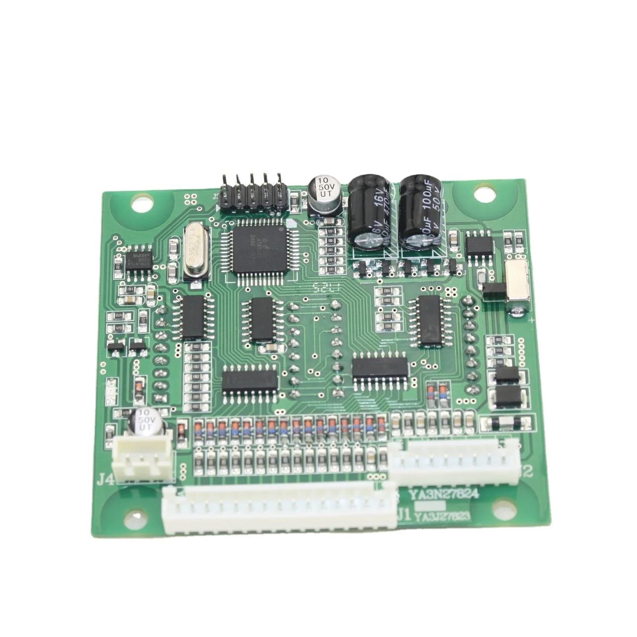
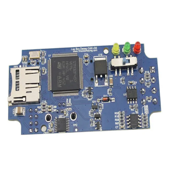
Smart Electric PCBA pcb board for dual ethernet custom multi layer printed circuit board
- Category: >>>
- Supplier: Shenzhen Moko Technology Ltd.
Share on (62091919642):
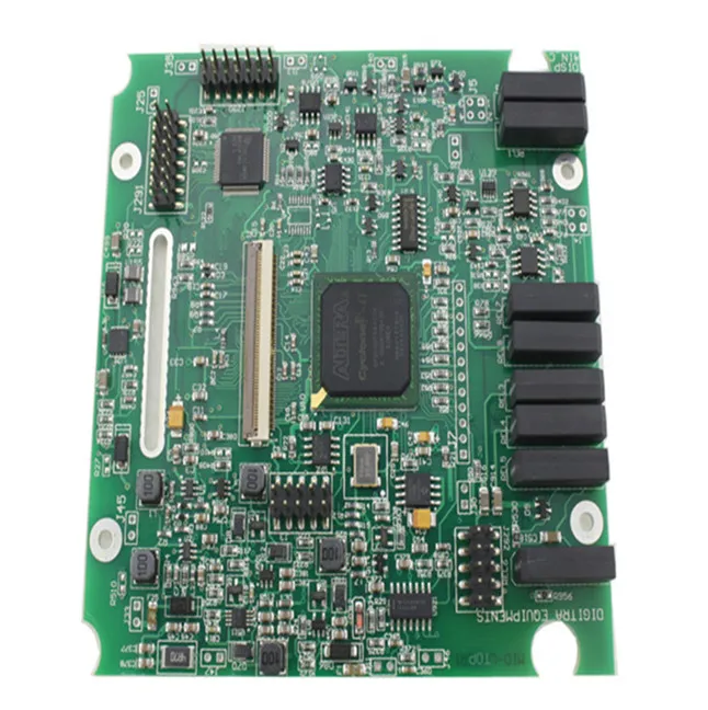
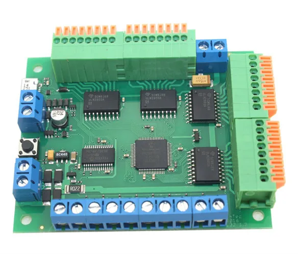
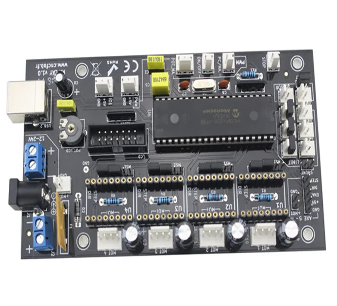
Product Overview
Description
Smart Electric PCBA pcb board for dual ethernet board custom multi-layer printed circuit board

Welcome To Moko
Founded in the year 2006,located in Shenzhen, as a professional EMS/OEM Manufacturer, MOKO TECHNOLOGY LTD could provide one-stop pcb assembly service,we also could offer:
- Contract Manufacturing
- Engineering Services
- PCB Assembly
- Component Procurement & Material Management
- Fast Track Prototyping
- Cable and Wire Assemblies
- Plastics and Molds
- Function Testing Service
As the Professional PCB Assembly and PCB Manufacturer in China, we pride ourselves on our Excellent Customer Service and Reliability! MOKO Technology Ltd also offers Exclusive Services to Help Our Customers with their PCB Projects.
Our Services
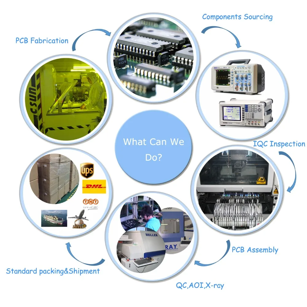
Our PCB Sevices:
1. PCB fabrication.
2. Turnkey PCBA: PCB+components+SMT and through-hole assembly+enclosure molding&housing.
Our Advantage:
1. Free programming and free functional test, free package.
2. High quality: IPC-A-610E standard, E-test, X-ray, AOI test, QC, 100% funtional test.
3. Professional service. ISO SMT and through hole assembly, over 10 years experience.
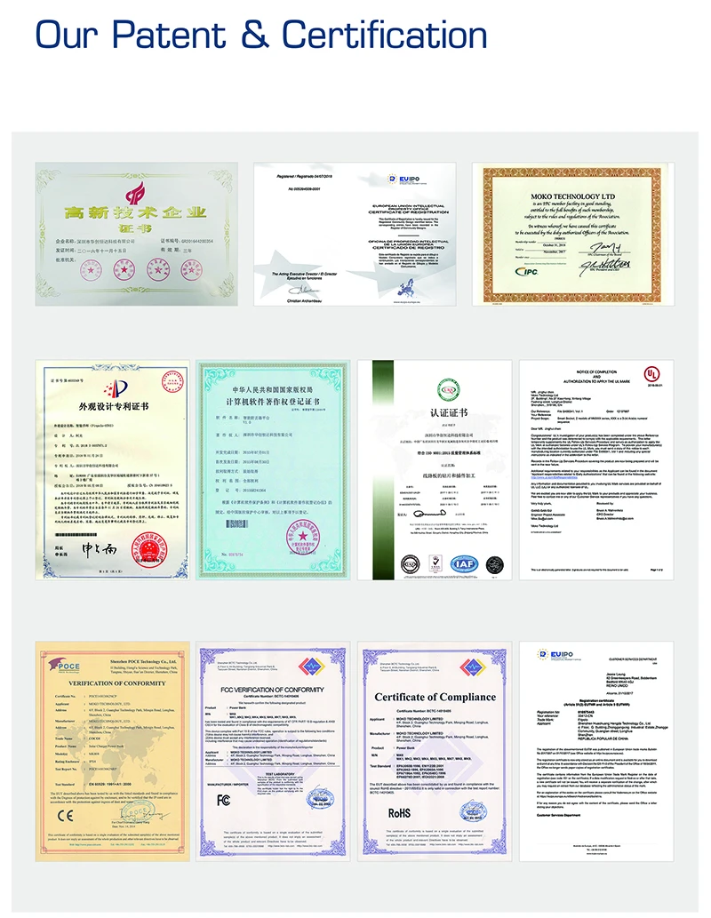
4. Certification for electronics: UL, 94v-0, CE, SGS, FCC, RoHS, ISO9001:2008, ISO14001
5. Warranty period for PCBA: 2 years.
| Turnkey PCBA | PCB+components sourcing+assembly+package |
| Assembly details | SMT and Thru-hole, ISO SMT and DIP lines |
| Lead Time | Prototype: 15 work days. Mass order: 20~25 work days |
| Testing on products | Flying Probe Test, X-ray Inspection, AOI Test, Functional test |
| Quantity | Min quantity: 1pcs. Prototype, small order, mass order, all OK |
| Files needed | PCB: Gerber files(CAM, PCB, PCBDOC) |
| Components: Bill of Materials(BOM list) | |
| Assembly: Pick-N-Place file | |
| PCB Panel Size | Min size: 0.25*0.25 inches(6*6mm) |
| Max size: 20*20 inches(500*500mm) | |
| PCB Solder Type | Water Soluble Solder Paste, RoHS lead free |
| Components details | Passive Down to 0201 size |
| BGA and VFBGA | |
| Leadless Chip Carriers/CSP | |
| Double-sided SMT Assembly | |
| Fine Pitch to 0.8mils | |
| BGA Repair and Reball | |
| Part Removal and Replacement | |
| Component package | Cut Tape,Tube,Reels,Loose Parts |
| PCB assembly process | Drilling-----Exposure-----Plating-----Etaching & Stripping-----Punching-----Electrical Testing-----SMT-----Wave Soldering-----Assembling-----ICT-----Function Testing-----Temperature & Humidity Testing |
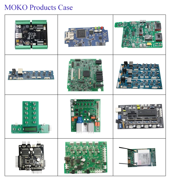
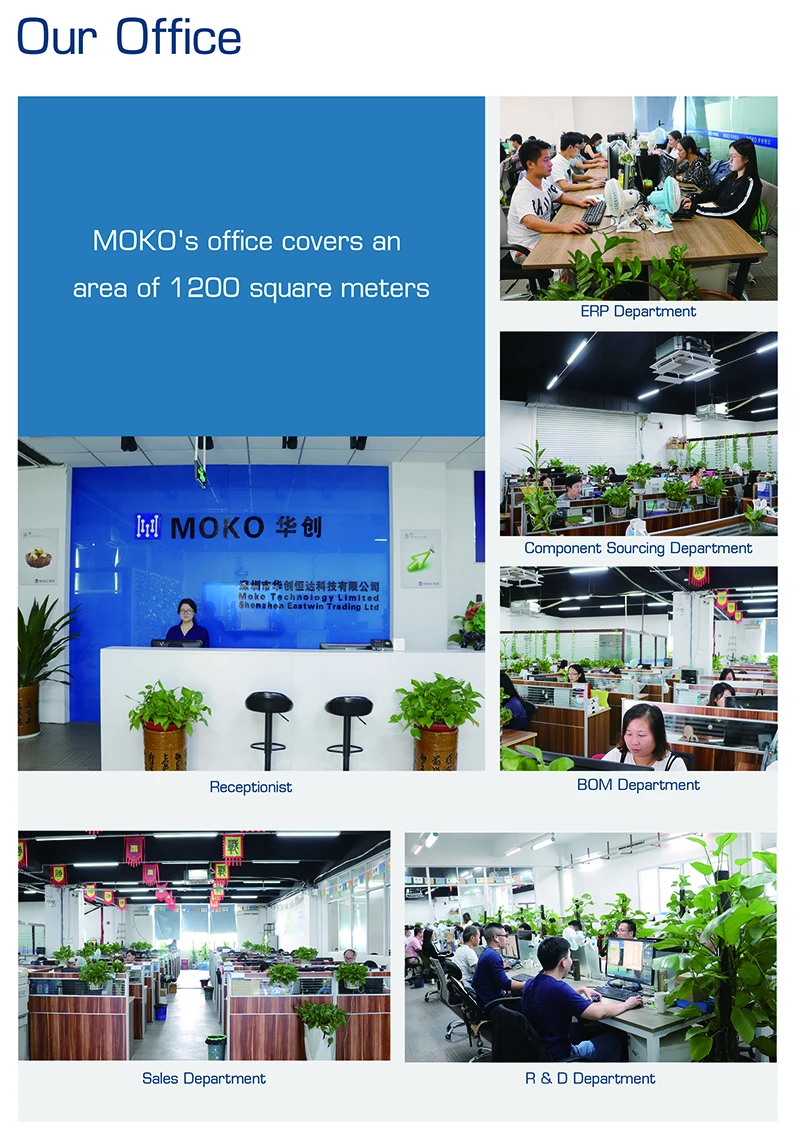
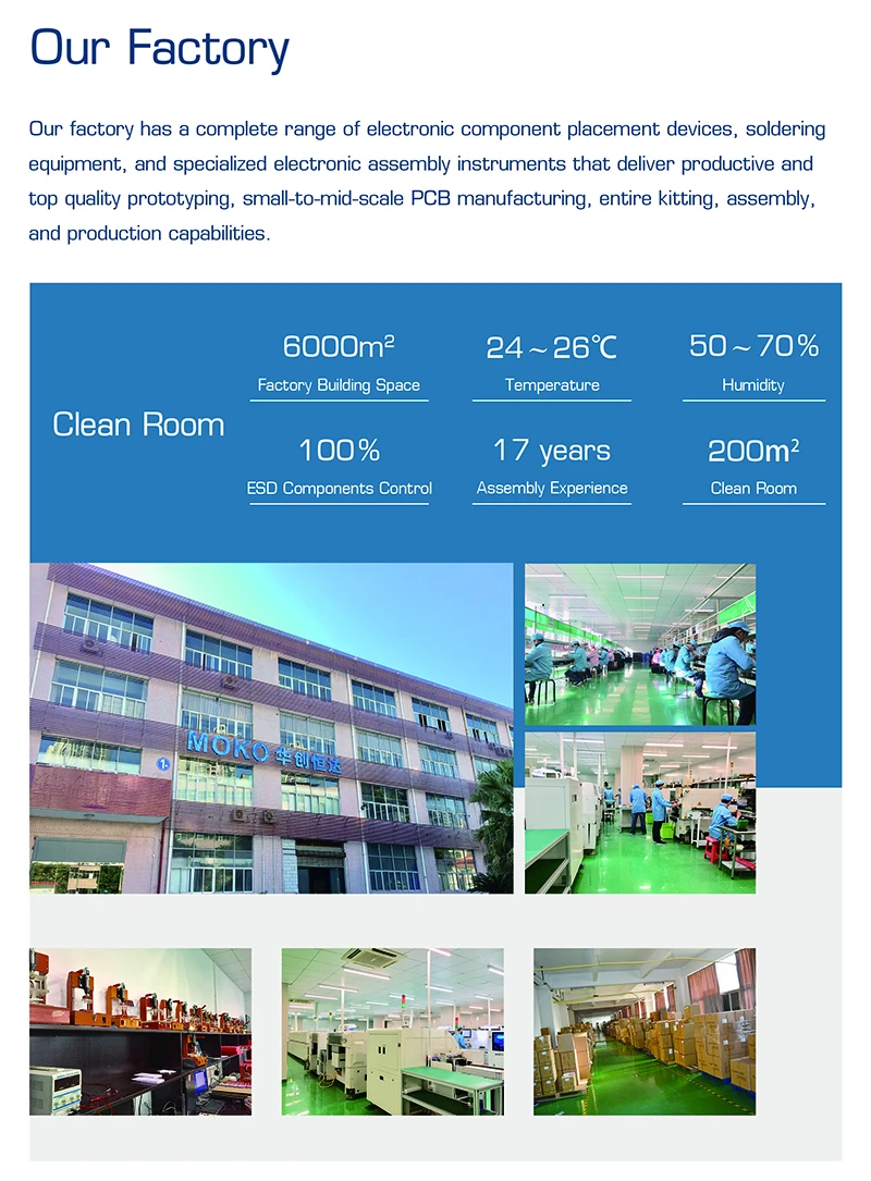
Company Information

FAQ
Q: What files do you use in PCBA fabrication?
A: Gerber or Eagle, BOM listing, PNP and Components Position
Q:Is it possible you could offer sample?
A: Yes, we can custom you sample to test before mass production
Q: When will I get the quotation after sent Gerber, BOM and test procedure?
A: Within 6 hours for PCB quotation and around 24 hours for PCBA quotation.
Q: How can I know the process of my PCBA production?
A: 7-10 days for PCB production and components purchasing, and 10 days for PCB assembly and Testing
Q: How can I make sure the quality of my PCBAs?
A: We ensure that each piece of PCBA products work well before shipping. We'll test all of them according to your test procedure. Also if there are any defect items during the shipping, we also can be free to repair for you.
Packaging & Shipping


We Recommend
New Arrivals
New products from manufacturers at wholesale prices


