We Know What You Need ! We understand your problems and can talk the language of your industry . Just talk to us , you can get benefits of our comprehensive fabrication know how , material features and problem-solving experiences .
Product Description
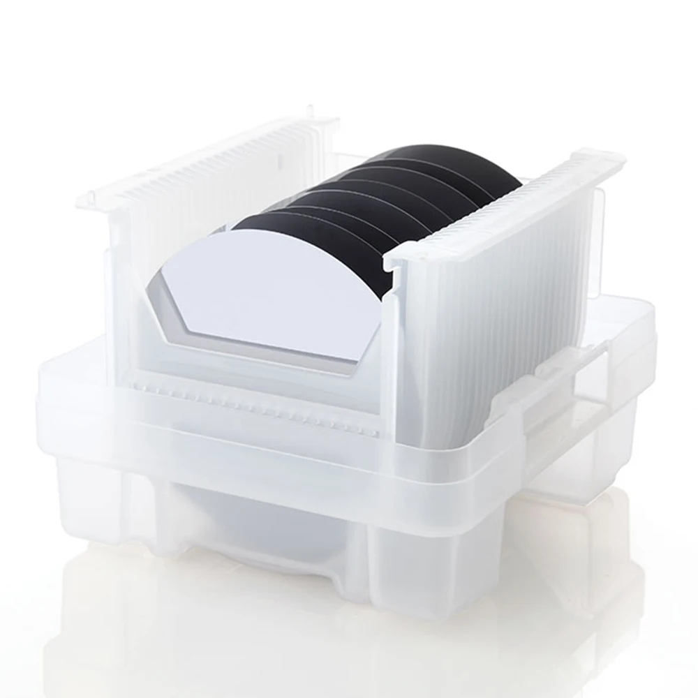
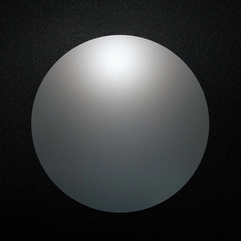
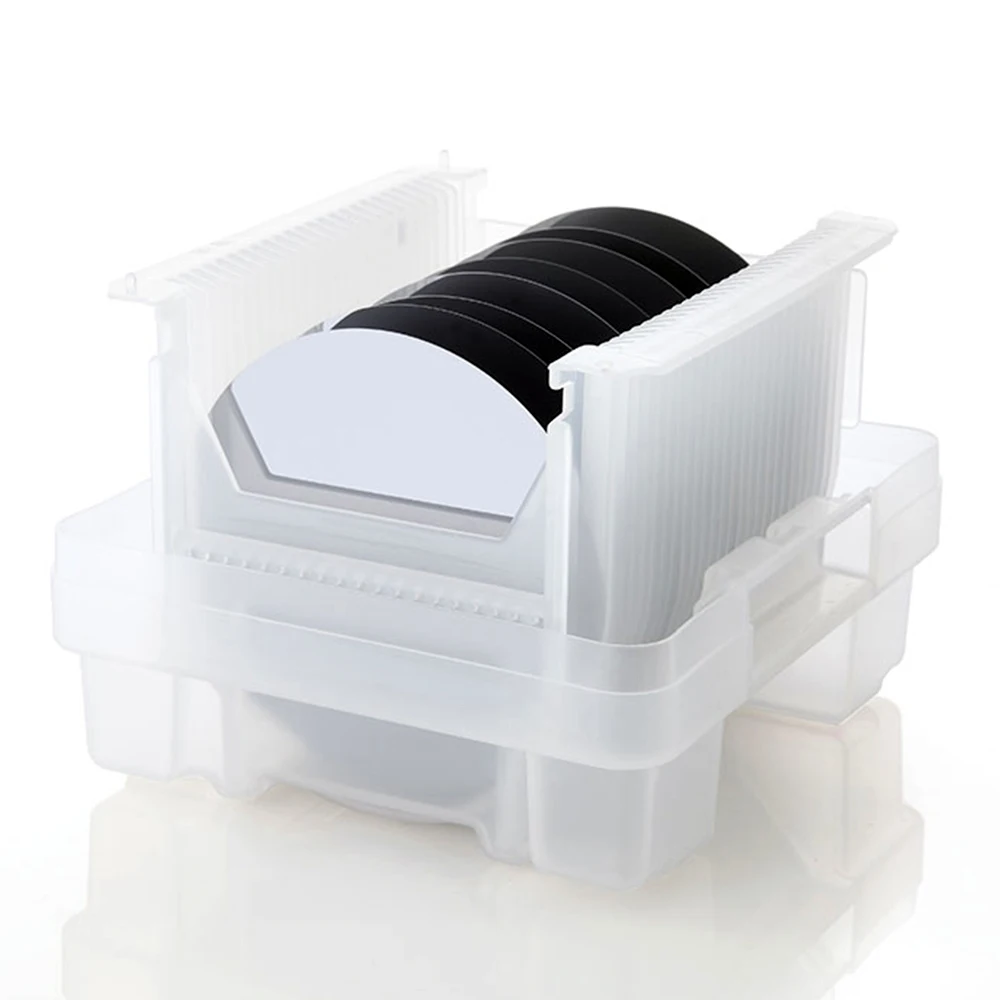
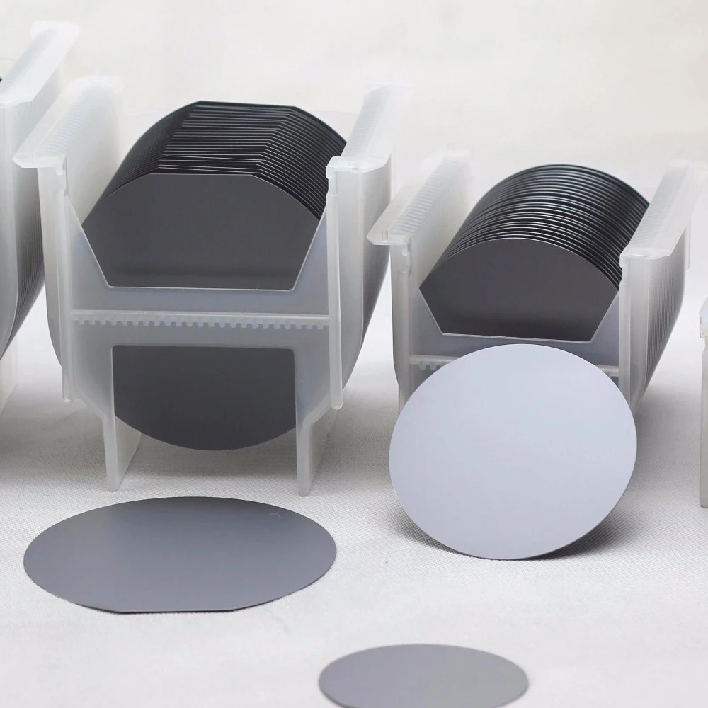
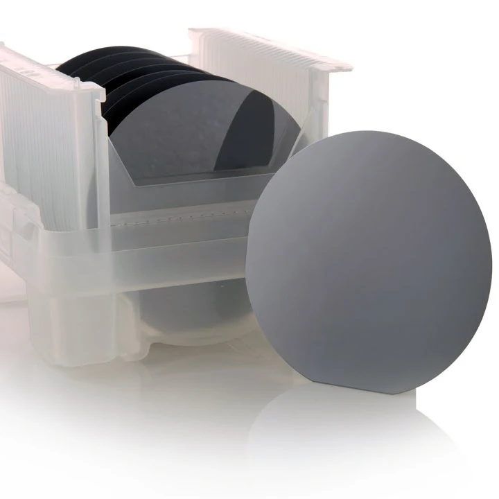
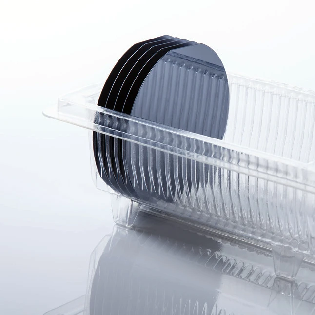
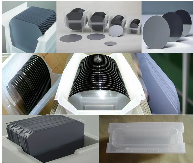
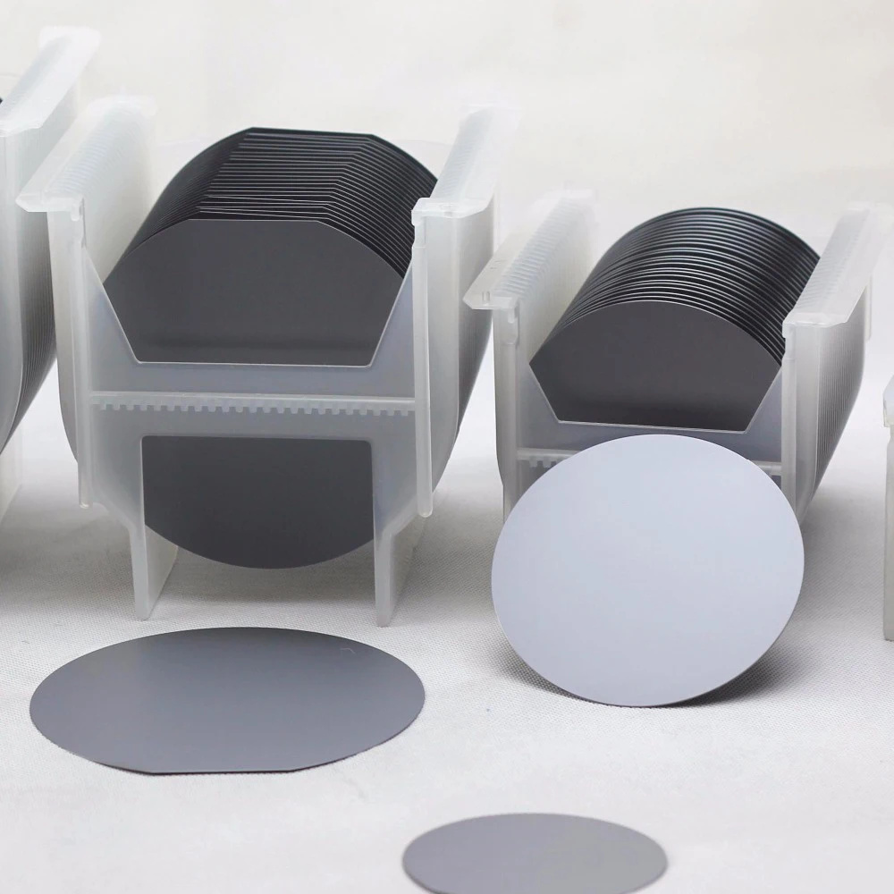
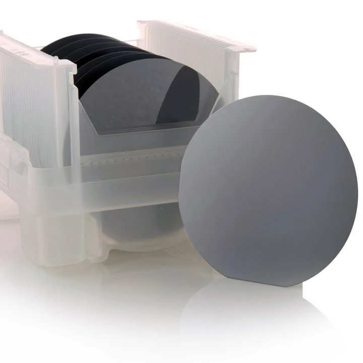
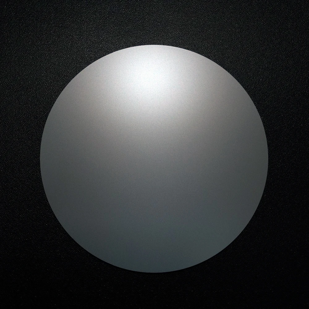
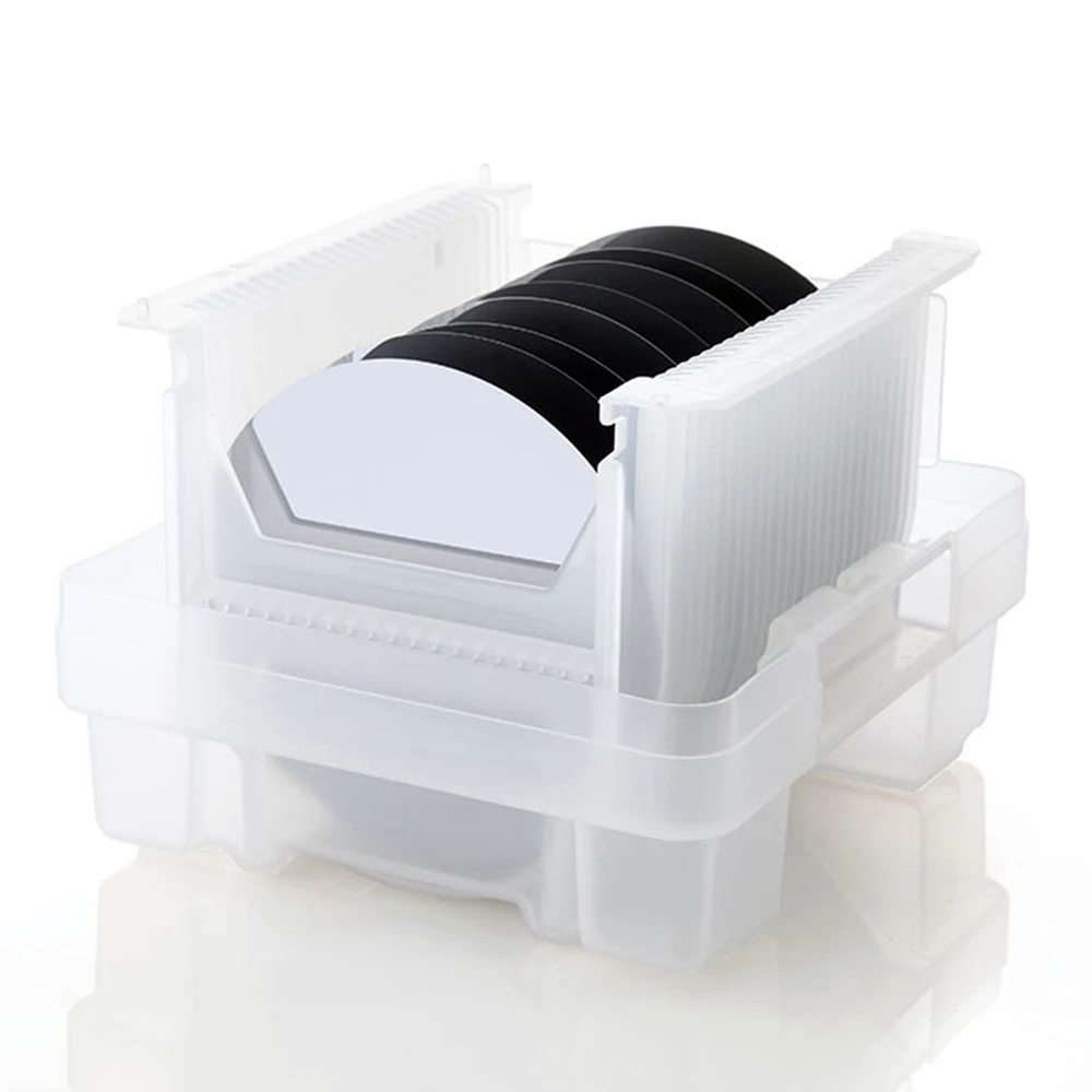
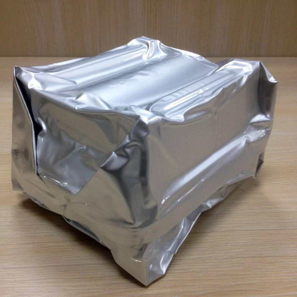
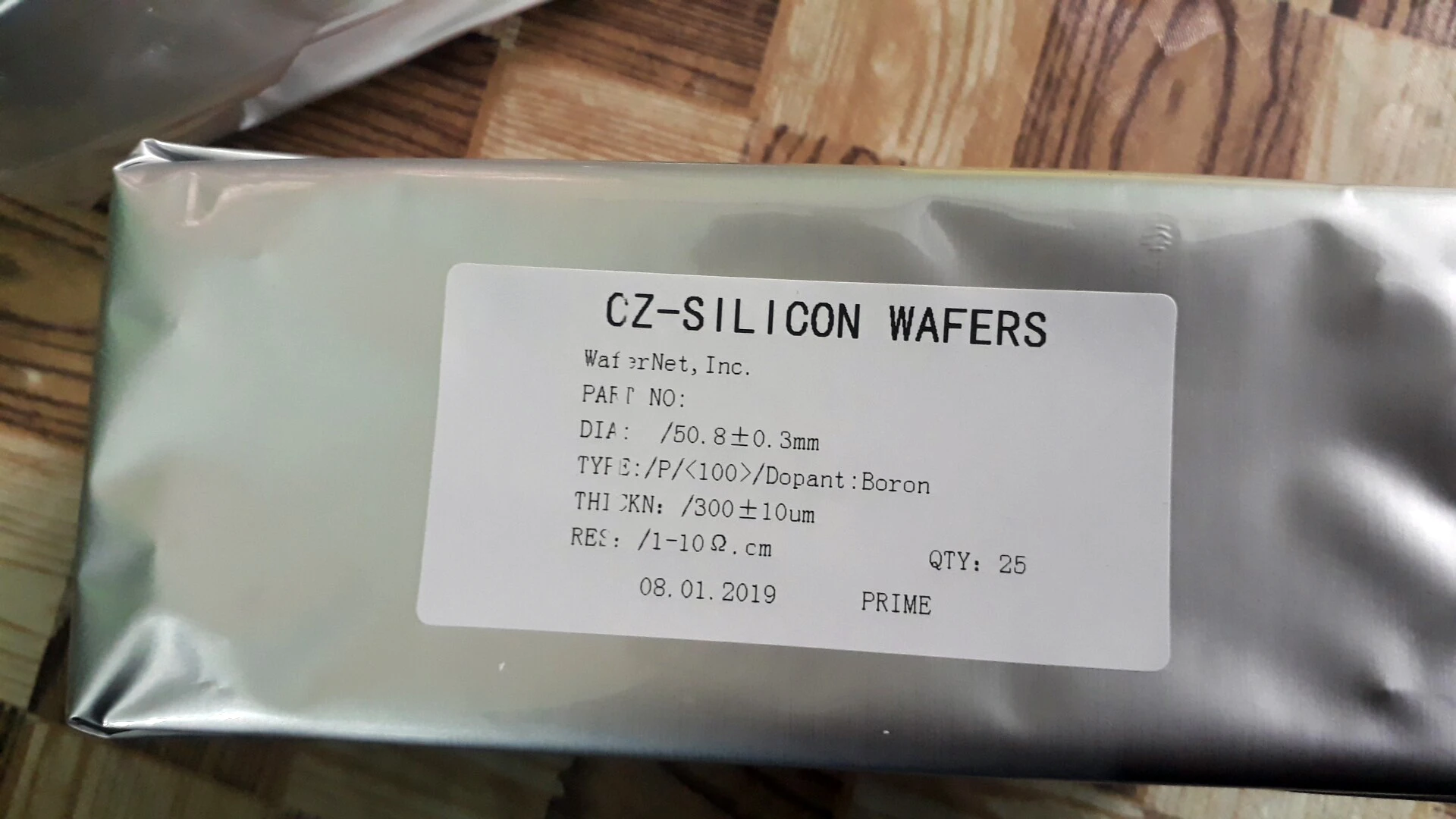
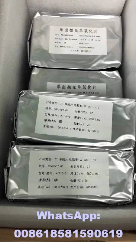
These 2" (50.8mm), 3" (76.2mm) and 4" (102mm) diameter silicon wafers can be used either as substrates for thin-film research or to make small silicon substrates by dicing the wafer into smaller pieces using a scriber. Wafers generally have flats or notches cut into one or more sides indicating the crystallographic plane and doping type. These silicon wafers are available as P-type (boron-doped) wafers which are cut with a primary flat. The wafers are 230 - 575µm thick polished on one side and do not have a silicon dioxide top coating. Each wafer is shipped in a wafer carrier.
Silicon Wafer Available
CZ or FZ Wafer
Prime Wafer
Intrinsic Wafer
Test Wafer
Heavily Doped Wafer
High Resistivity Wafer
Off Axis Orientation Wafer
Special Orientation Wafer
Ultra Flat Wafer
Ultra Thin Wafer
Ultra Thick Wafer
Double Sides Polished
Thermal Oxide Wafer
Epi Wafer
Product Specification
Growth
CZ / FZ
Diameter
Ø 2" / Ø 3" / Ø 4" / Ø 6" / Ø 8" / Ø 12"
Thickness
275 um ~ 775 um
Orientation
<100> / <111> / <110> or others
Conductivity
P - type / N - type / intrinsic
Dopant
Boron / Phosphorous / Antimony / Arsenic
Resistivity
0.001 ~ 10000 ohm-cm
Surface
One side polished / two sides polished
TTV
<= 10 um
Bow / Warp
<= 40 um
Grade
Prime / Test / Dummy grade
Detailed Images
FAQ
Q: What's the way of shipping and cost?
A:(1) We accept DHL, Fedex, TNT, UPS, EMS etc.
(2) If you have your own express account, it's great.If not,we could help you ship them. Freight is USD30
Q: How to pay?
A: T/T, Paypal, Secure payment and Assurance payment on Alibaba.com and etc..
Q: What's your MOQ?
A: (1) For inventory, the MOQ is 25pcs/Box.
(2) For customized products, the MOQ is 50pcs.
Q: What's the delivery time?
A: (1) For the standard products
For inventory: the delivery is 5 workdays after you place the order.
For customized products: the delivery is 2 or 3 weeks after you place the order.
(2) For the special-shaped products, the delivery is 4 or 6 workweeks after you place the order.
Q: Do you have standard products?
A: Our standard products in stock.
Q: Can I customize the products based on my need?
A: Yes, we can customize the material, specifications and optical coating for your optical components based on your needs.
Q: Do you have inspection report for material?
A: We can supply ISO,CE etc for our products.
Q: How to ensure the safety of payment?
A: We are the gold supplier on alibaba.com and supports Alibaba Trade Assurance.
Contact Us
Please send us an inquiry, tell us your requirements, we will reply to you in 3hours.