
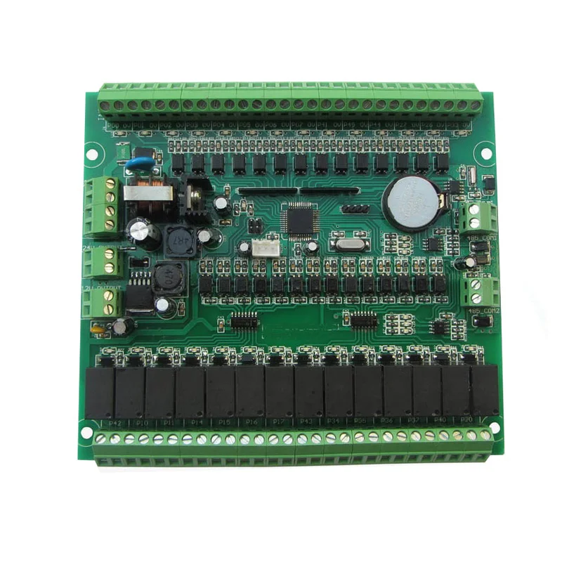
Moko smart home control panel board assembly
- Category: >>>
- Supplier: Shenzhen Moko Technology Ltd.
Share on (62270008969):
Product Overview
Description
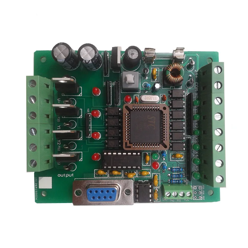
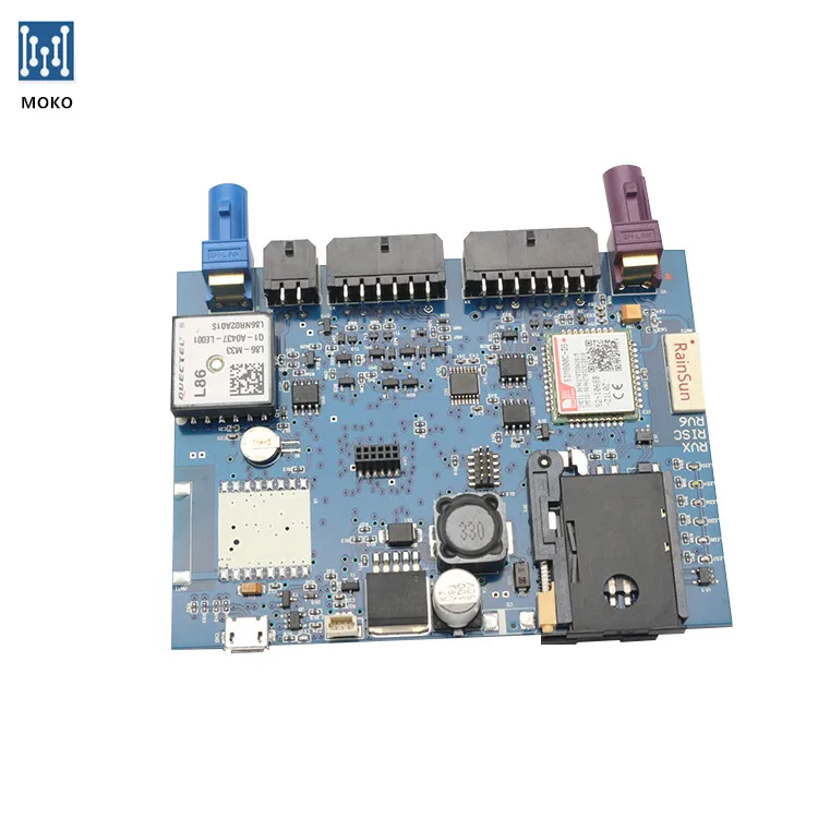
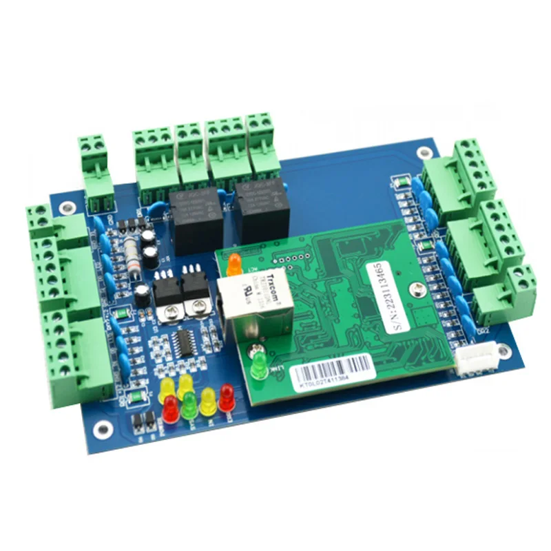
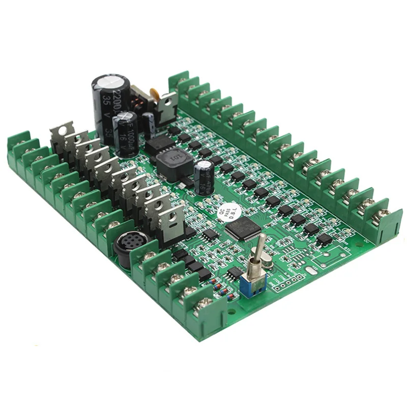
Moko smart home solution control panel board assembly


Product Description
1.OEM/ODM/EMS services
* High quality printed circuit board assembly
* Fast FR4 PCB Fabrication
* NO MOQ requirement
* NO MOQ requirement
* RoHS compliant, lead-free
* Fast delivery, anti-static package
* Fast delivery, anti-static package
* Final functional test for free
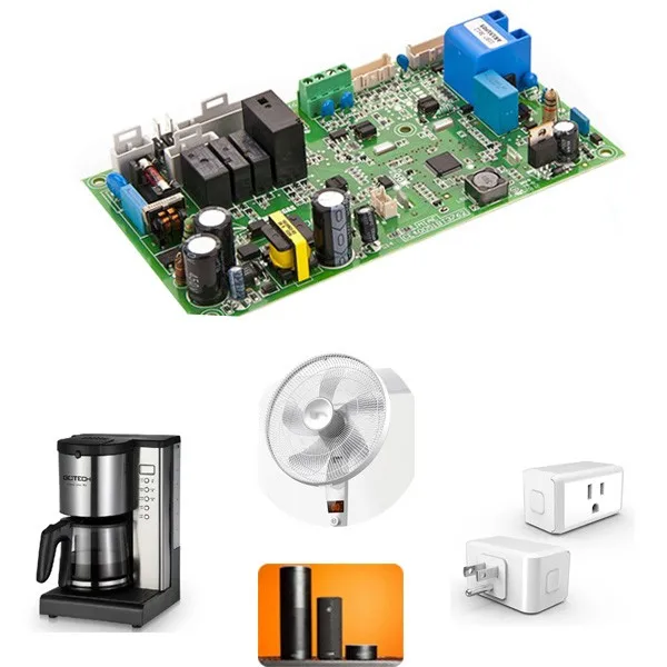
* Custom pcbs is widely used in the area of IoT, smart home, power control, wireless and RF, Medical devices
2. Detailed terms for PCB assembly:
1. Professional surface-mounting and through-hole soldering technology
2. ICT (in circuit test), FCT (functional circuit test) technology.
3. PCB assembly with UL, CE, FCC, RoHS approval
4. Nitrogen gas reflow soldering technology for SMT
5. High standard SMT and solder assembly line
6. Cable & wiress assembly, full box build assembly
2. ICT (in circuit test), FCT (functional circuit test) technology.
3. PCB assembly with UL, CE, FCC, RoHS approval
4. Nitrogen gas reflow soldering technology for SMT
5. High standard SMT and solder assembly line
6. Cable & wiress assembly, full box build assembly

PCBA PROCESSING CAPABILITY :
| Turnkey PCBA | PCB+components sourcing+assembly+package |
| Assembly details | SMT and Thru-hole, ISO SMT and DIP lines |
| Lead Time | Prototype: 15 work days. Mass order: 20~25 work days |
| Testing on products | X-ray Inspection, AOI Test, Functional test |
| Quantity | Min quantity: 1pcs. Prototype, small order, mass order, all OK |
| Files needed | PCB: Gerber files(CAM, PCB, PCBDOC) |
| Components: Bill of Materials(BOM list) | |
| Assembly: Pick-N-Place file | |
| PCB Panel Size | Min size: 0.25*0.25 inches(6*6mm) |
| Max size: 20*20 inches(500*500mm) | |
| PCB Solder Type | Water Soluble Solder Paste, RoHS lead free |
| Components details | Passive Down to 0201 size |
| BGA and VFBGA | |
| Leadless Chip Carriers/CSP | |
| Double-sided SMT Assembly | |
| Fine Pitch to 0.8mils | |
| BGA Repair and Reball | |
| Part Removal and Replacement | |
| Component package | Cut Tape,Tube,Reels,Loose Parts |
PCB PROCESSING CAPABILITY :
| 1 | Layers | Single Sided,2 to 18 Layer |
| 2 | Board material type | FR4,CEM-1,CEM-3,ceramic substrate board, aluminum based board, high-Tg, Rogers and more |
| 3 | Compound material lamination | 4 to 6 layers |
| 4 | Maximum dimension | 610 x 1,100mm |
| 5 | Dimension tolerance | ±0.13mm |
| 6 | Board thickness coverage | 0.2 to 6.00mm |
| 7 | Board thickness tolerance | ±10% |
| 8 | DK thickness | 0.076 to 6.00mm |
| 9 | Minimum line width | 0.10mm |
| 10 | Minimum line space | 0.10mm |
| 11 | Outer layer copper thickness | 8.75 to 175µm |
| 12 | Inner layer copper thickness | 17.5 to 175µm |
| 13 | Drilling hole diameter (mechanical drill) | 0.25 to 6.00mm |
| 14 | Finished hole diameter (mechanical drill) | 0.20 to 6.00mm |
| 15 | Hole diameter tolerance (mechanical drill) | 0.05mm |
| 16 | Hole position tolerance (mechanical drill) | 0.075mm |
| 17 | Laser drill hole size | 0.10mm |
| 18 | Board thickness and hole diameter ratio | 10:1 |
| 19 | Solder mask type | Green, Yellow, Black, Purple, Blue, White and Red |
| 20 | Minimum solder mask | Ø0.10mm |
| 21 | Minimum size of solder mask separation ring | 0.05mm |
| 22 | Solder mask oil plug hole diameter | 0.25 to 0.60mm |
| 23 | Impedance control tolerance | ±10% |
| 24 | Surface finish | Hot air level, ENIG, immersion silver, gold plating, immersion tin and gold finger |
PCB LEAD TIME
Layer Details | Sample(Normal) | Sample(Fast) | Mass Production |
Single/Double | 2-3days | 24hours | 5-7days |
Four Layer | 7-10days | 3days | 7-10days |
Six-Eight Layer | 7-10days | 5days | 13-15days |
Over Eight Layer | 15-20days | 7days | 15-20days |
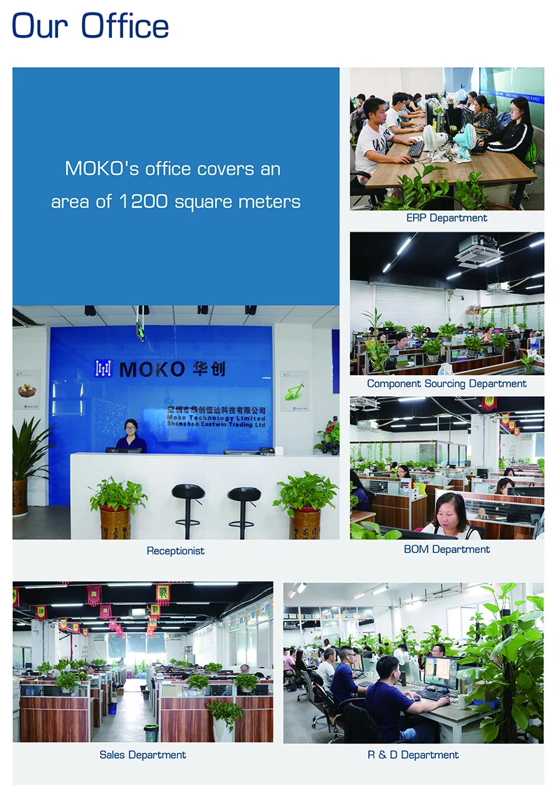
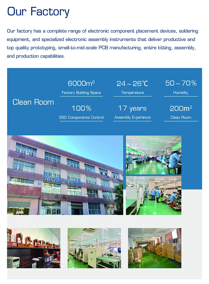
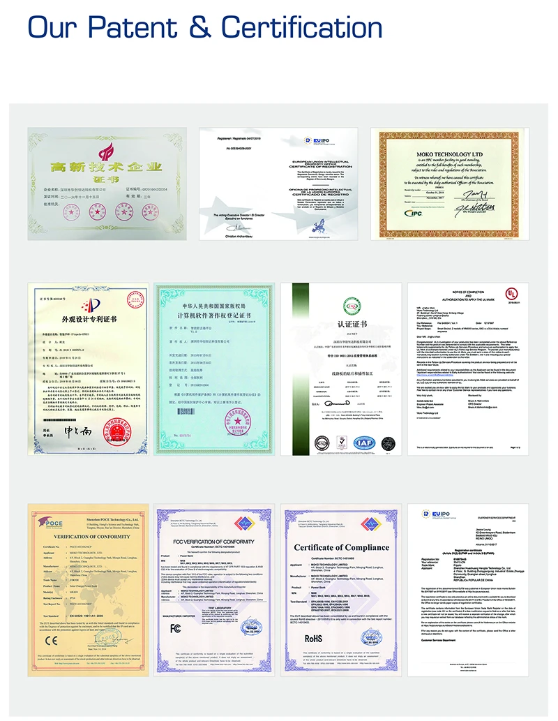
Company Information


FAQ
Q: What files do you use in PCBA fabrication?
A: Gerber or Eagle, BOM listing, PNP and Components Position
Q:Is it possible you could offer sample?
A: Yes, we can custom you sample to test before mass production
Q: When will I get the quotation after sent Gerber, BOM and test procedure?
A: Within 6 hours for PCB quotation and around 24 hours for PCBA quotation.
Q: How can I know the process of my PCBA production?
A: 7-10 days for PCB production and components purchasing, and 10 days for PCB assembly and Testing
Q: How can I make sure the quality of my PCBAs?
A: We ensure that each piece of PCBA products work well before shipping. We'll test all of them according to your test procedure. Also if there are any defect items during the shipping, we also can be free to repair for you.
Packaging & Shipping

We Recommend
New Arrivals
New products from manufacturers at wholesale prices


