
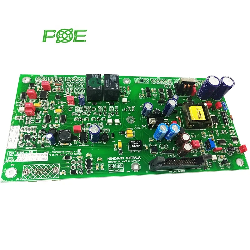
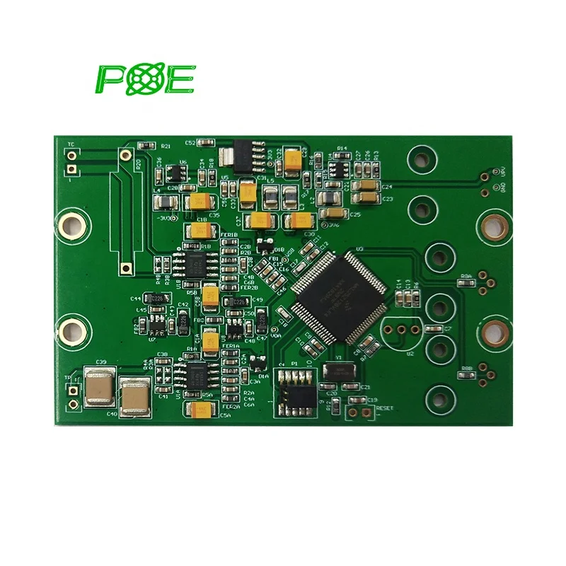
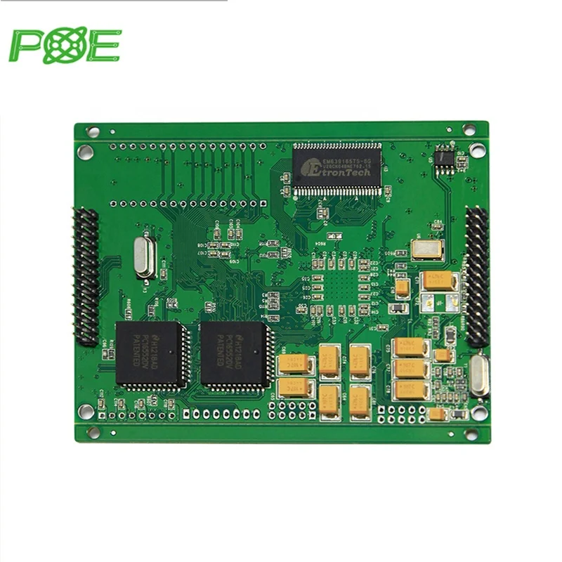
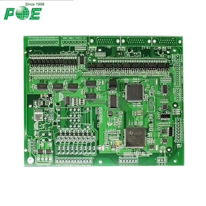
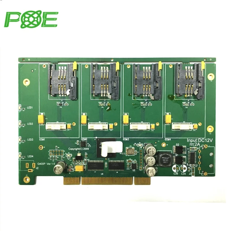
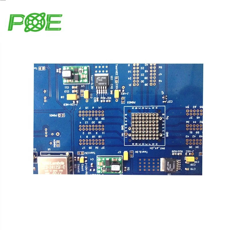
Top Quality Electronic Pcb Assembly Pcba Pure Sine Wave Inverter Pcb Circuit Board Supplier
- Category: PCBA >>>
- Supplier: Shenzhen POE Precision Technology Co. Ltd.
Share on (62407510006):
Product Overview
Description


Item | PCB/PCBA/FPCB |
Finished surface | Conventional HASL, Lead-free HASL, Falsh Gold, ENIG(Immersion Gold), Osp, Immersion Tin, Immersion Silve |
Base Material | FR-4(shengyi China, TEQ, KB A+. HZ))/ High TG FR-4 / Rgon/sola//Rogers/Arlon/Taconic/Teflon |
Layers | 1-40 |
Finised inner/outer copper thickness | 0.5-6OZ |
Finished board thickness | 0.2-7.0mm |
Technical specification | Min line width/gap: 3.5/4mil(laser drill) Min hole size: 0.15mm Min Annular ring: 4mil Max copper thickness: 6OZ Max production size: 900*1200mm Board thickness: D/S: 0.2-7.0mm, multilayers: 0.40-7.0mm Min solder mask bridge: ≥0.08mm Aspect ratio: 15:1 Plugging Visa capability: 0.2-0.8mm |
Controlled Impedance | +/-5% |
Plugging vias capability | 0.2-0.8mm |
Outline profile | Rout/ V-cut/ Bridge/ Stamp hole |
Tolerance | Plated holes Tolerance: ±0.08mm(min±0.05) Non-plated hole tolerance: ±0.05mm(min+0/-0.05mm or +0.05/-0mm) Outline tolerance: ±0.15mm(min±0.10mm) Functional test: Insulating resistance: 50ohms Peel off strength: 1.4N/mm Thermal stress test: 2650c, 20 seconds Solder mask hardness: 6HE-test voltage: ≥00V+15/-0v 30s Warp and twist: 0.7%(semiconductor test board ≤.3%) |


1.POE use Panel plating for copper sinking process, what is the benefits by using Panel plating?
As we can see, the N-layer inner circuit can be connected to the outer circuit in multilayer PCB,the copper sinking process uses the metal palladium (Pd) adsorption hole wall to connect with the inner circuit to achieve conductivity. This process is complicated to produce and the palladium metal is expensive (50% dearer than gold), but the reliability is high and the serve-life is long. Generally, large high-end factories only use this process.
2. How to recognize Electroless Plating Copper (PTH) and Conductive Adhesive?
Conductive Adhesive also called black hole, it can be found on the NPTH hole wall. The color of panel plating copper is the fiber substrate itself, and the Conductive Adhesive has a
black glue attached to the hole wall.
black glue attached to the hole wall.


Feedback

Product packaging

Q1: What is needed for PCB PCBA quotation?
PCB(printed circuit board): Quantity, Gerber file and Technic requirements(material,surface finish treatment,
copper thickness,board thickness ,...)
PCBA(printed circuit board assembly): PCB information, BOM, (Testing documents...)
Q2: What file formats do you accept for PCB PCBA production?
Gerber file: CAM350 RS274X
PCB file: Protel 99SE, P-CAD 2001 PCB
BOM: Excel (PDF,word,txt)
Q3: Are my files safe?
Your files are held in complete safety and security. We protect the intellectual property for our customers in the whole process. All documents from customers are never shared with any third parties.
Q4: MOQ?
There is no MOQ in POE(pcba shenzhen). We are able to handle Small as well as large volume production with flexibility.
Q5: Shipping cost?
The shipping cost is determined by the destination, weight, packing size of the goods. Please let us know if you need us to
quote you the shipping cost.
We Recommend


New Arrivals
New products from manufacturers at wholesale prices


