
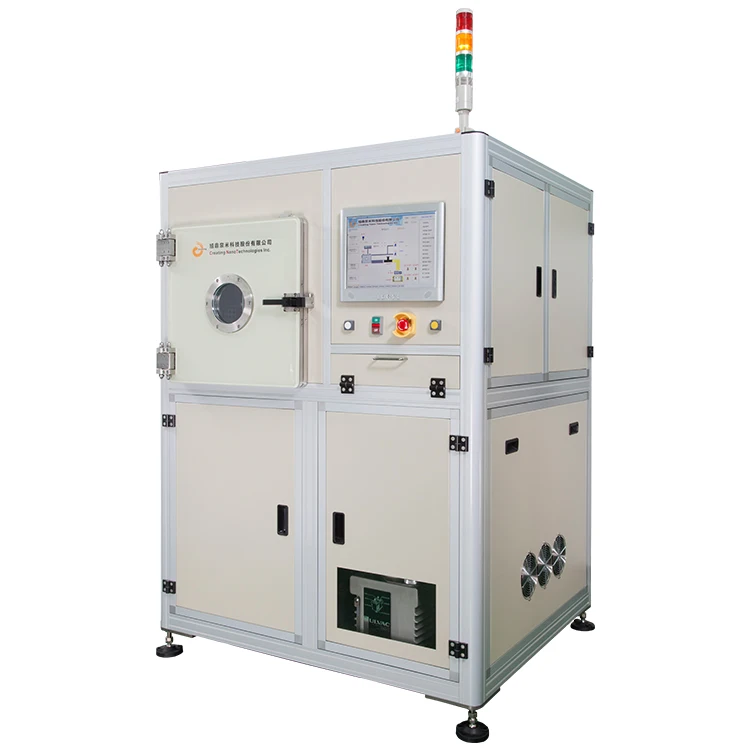
Vacuum Plasma Asher painting, gluing or bonding
- Category: >>>
- Supplier: CREATING NANO TECHNOLOGIES INC.
Share on (62407876966):
Product Overview
Description
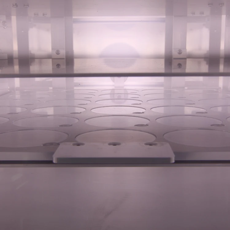
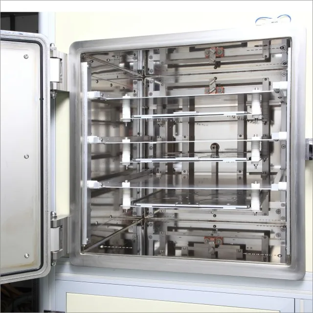
Product Description
Production Description
Product Features
Related solutions
Specification


Award


The exhibition


Q: Are you trading company or manufacturer?
A: We have our own Equipment factories.
Q: Why choose us?
A: We have a lot of experience, enable us to suggest you the best solution.
Q: How do you make our business long-term and good relationship?
A:1. We keep good quality and competitive price to ensure our customers benefit ;
2. We respect every customer as our friend and we sincerely do business and make friends with them,
no matter where they come from.
We Recommend

New Arrivals
New products from manufacturers at wholesale prices


