


Высокое качество Электронный Pcb дизайн программного обеспечения PCB платы приложения
- Категория: Computer & Information Technology Services >>>
- Поставщик: Dalian Jinseo Electronic Technology Co. Ltd.
Сохранить в закладки 1600185545221:
Описание и отзывы
Характеристики

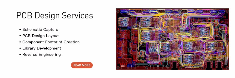
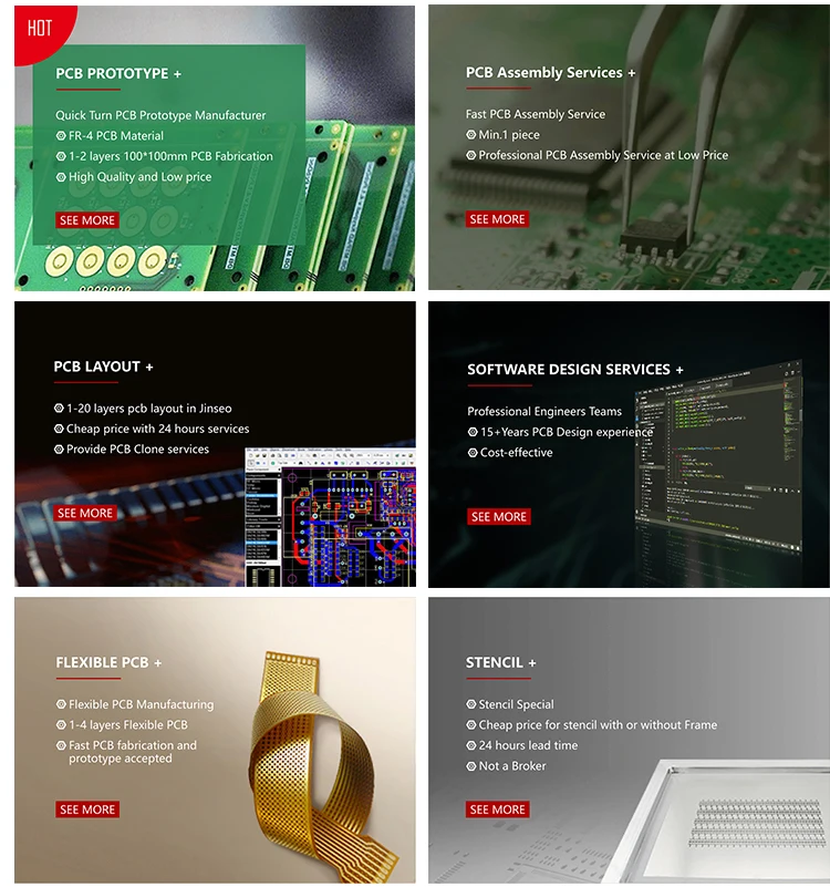
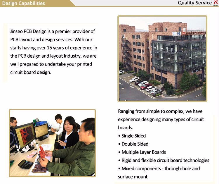


JINSEO PCB Design has the ability to complete your schematic capture and PCB layout in several different software packages including: • Cadence OrCAD/Allegro • Altium PCAD • Altium Designer |


• Acquire all information needed, reviewing and verifying the accuracy. • Schematic capture and net list generation (if not done yet). • Create part library for the project. • PCB component placement. • Submit intermediate placement to engineer for reviewing. This is usually a discussion- modification process until get approval on final placement. • PCB routing. PCB designer and engineer must maintain adequate and frequent communication during the routing process. • Complete PCB layout, finalize all documents.
|

• Bill Of Materials (BOM). • Final Net list. • Hardcopy (or electronic version) of Schematics. • Data sheets for special parts, if any. • Any special instructions on layer stack-up (i.e. Signal, Ground & Power Planes) and plane splitting. • Any drawing/detailed scratch showing board shape, size, and mounting mechanism, or heat sink, etc. • Silkscreen text identification, including Part Numbers and Revisions. • Any signals requiring special routing. • Any placement requirements or restrictions (Placement ideas is greatly helpful). |

• PCB Design Files. • Standard PCB fabrication files (Gerber & NC-Drill in standard formats). • Schematics and BOM if the schematic capture process involved in the design order. • Assembly drawings. • Assembly machine pick-place data file. • Solder paste stencil files. • Other optional files as client required. |

• Provide as accurate information of circuit design and system requirement as possible. • Avoid/minimize change on schematic after PCB layout process begins. • Reducing density and making practical requirement. • Choose responsible and highly skilled PCB designers. |
• Schematics and BOM if the schematic capture process involved in the design order.
• Assembly drawings.
• Assembly machine pick-place data file.
• Solder paste stencil files.
• Other optional files as client required.
• Provide as accurate information of circuit design and system requirement as possible. • Avoid/minimize change on schematic after PCB layout process begins. • Reducing density and making practical requirement. • Choose responsible and highly skilled PCB designers. |
Похожие товары

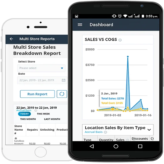
Лучшая компания по разработке мобильных приложений с опытными программаторами мобильных приложений
Мобильное приложение для заживления лечебных ударов ASMR для возрастной интенсивности упражнений
14,99 $
Разработка программного обеспечения посещаемости
10,00 $
Приложение для ремонта мобильного телефона
Лучший онлайн-сайт электронной коммерции с интегрированными услугами платежного шлюза
Проектирование программного обеспечения, лучшие услуги по проектированию программного обеспечения, программного обеспечения, решения для систем программного обеспечения, разработанные компанией ProtoLabz
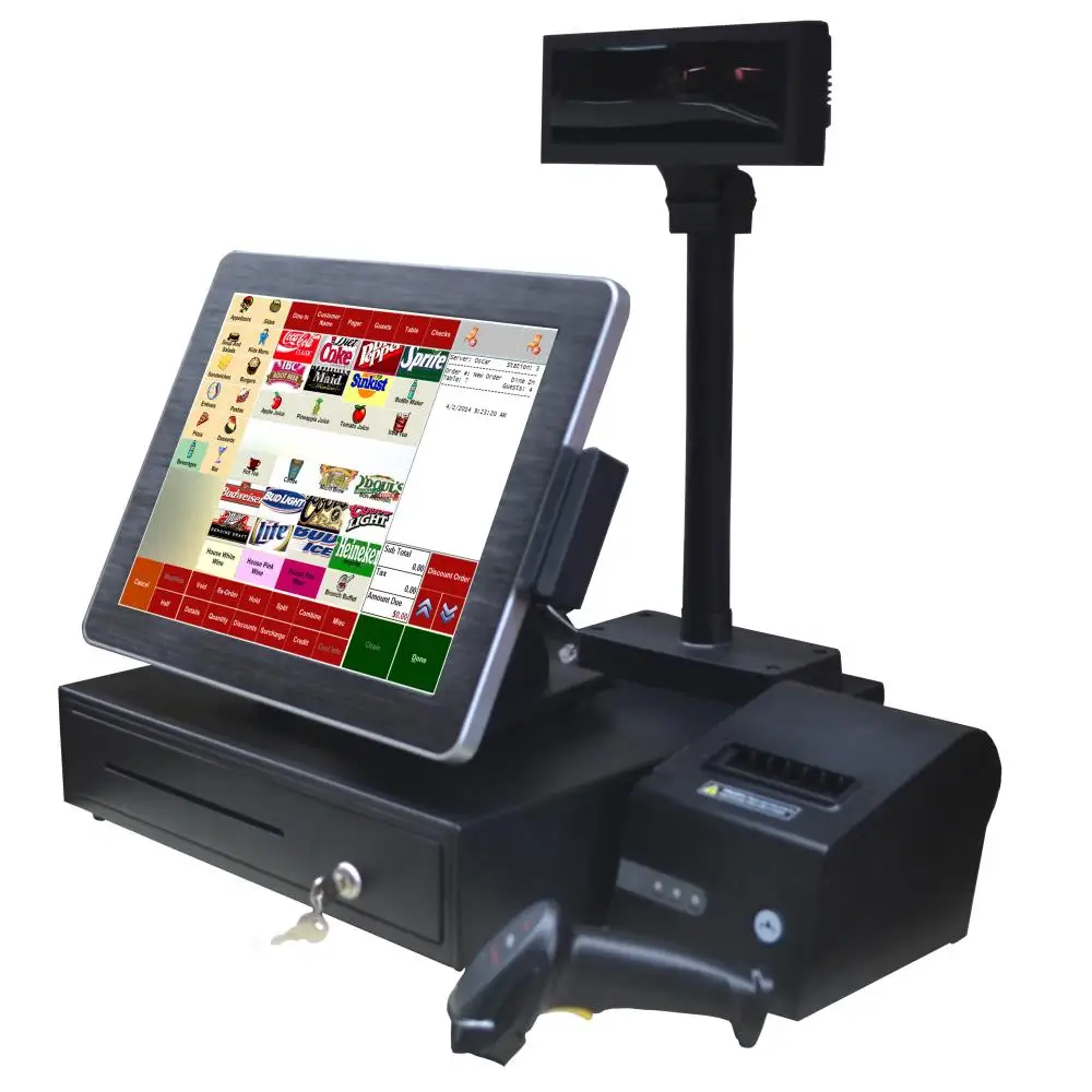
Программное обеспечение POS
Новые поступления
Новинки товаров от производителей по оптовым ценам
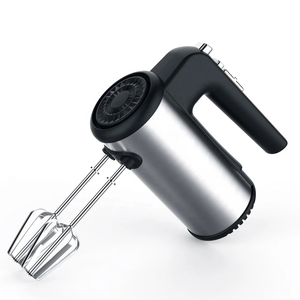
300 Вт безопасный для посудомоечной машины 5-скоростной турбо с крючками для теста, венчик, электрический ручной миксер
571,11-666,30 ₽
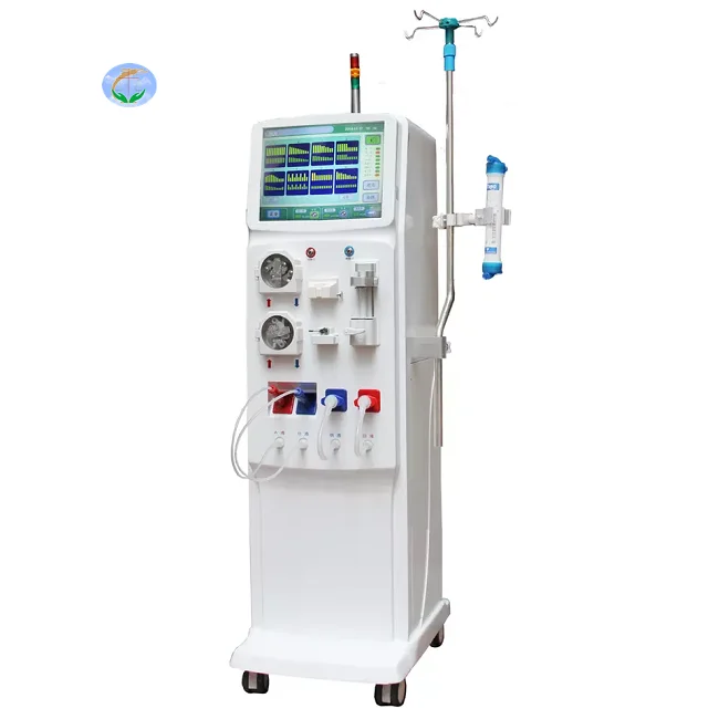
Медицинский портативный прибор для гемодиализа катетер и кровообращения диализа почек ухода за здоровьем
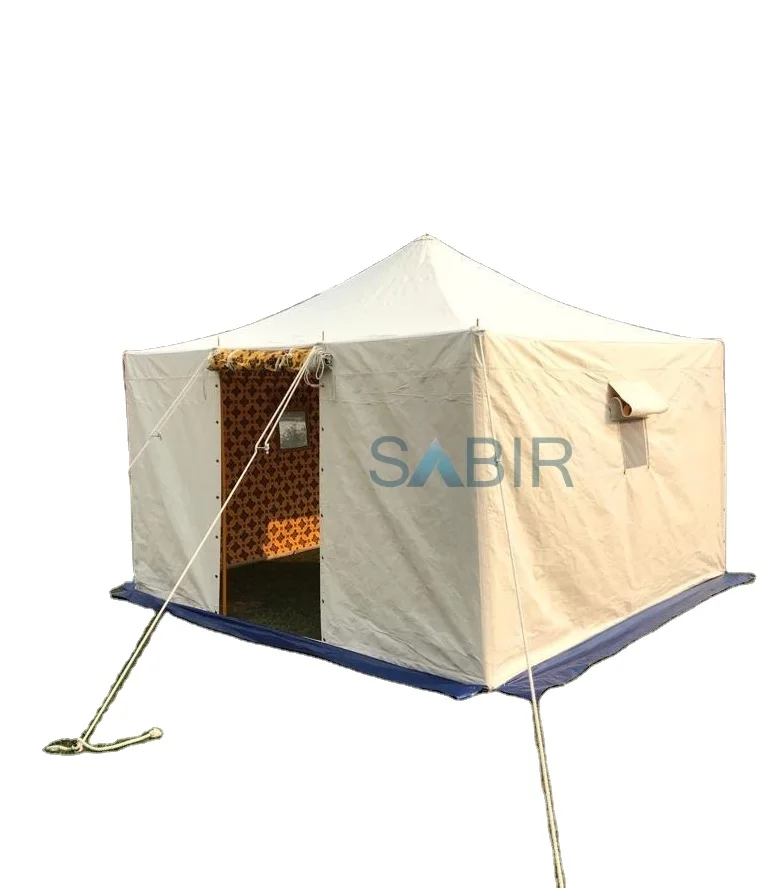
Многофункциональная роскошная водонепроницаемая палатка из брезента для кемпинга однокомнатная всесезонная с настраиваемым размером новый стиль рынка Ближнего Востока
45 688,76-56 159,10 ₽
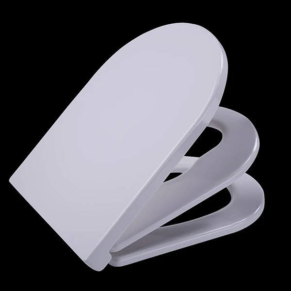
Санитарно-гигиеническое сиденье для
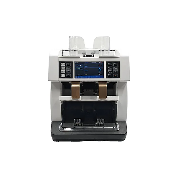
Счетчик купюр с низким уровнем шума на тонкопленочных транзисторах, автоматическое определение разных валют, 4,2 дюйма
50 448-52 351,70 ₽
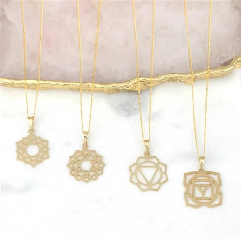
Ожерелье из нержавеющей стали изящное ожерелье с чакрами на заказ модное позолоченное ювелирное изделие водонепроницаемой подвеской без
121,84-217,03 ₽
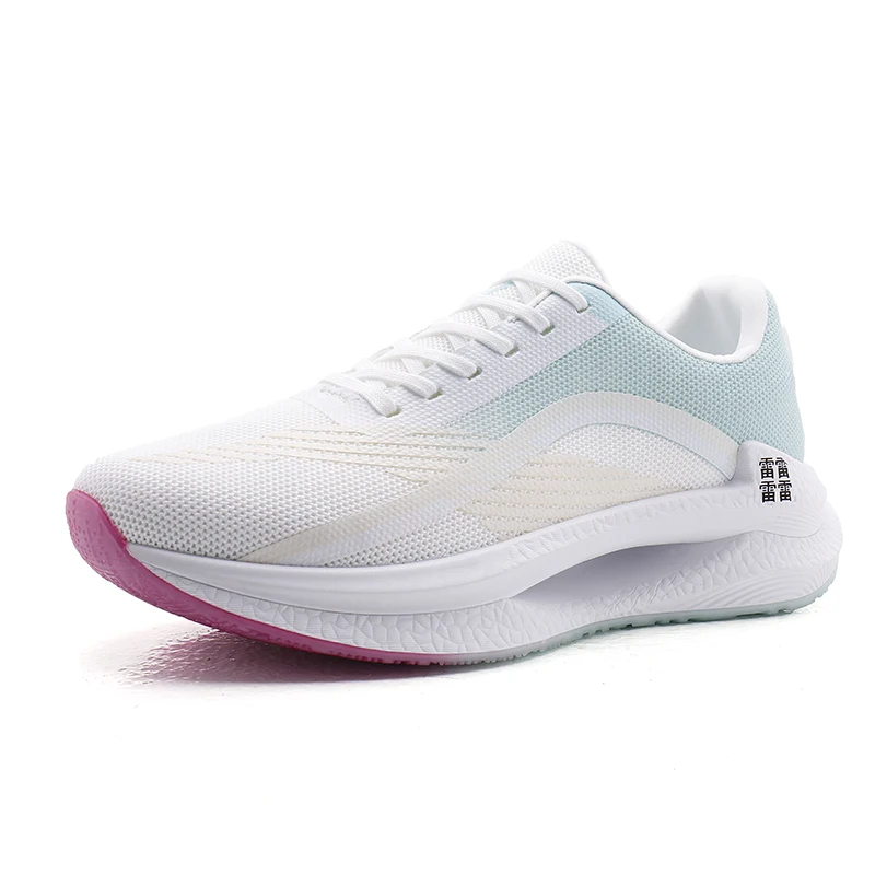
Мужские спортивные кроссовки с логотипом
856,67-999,45 ₽
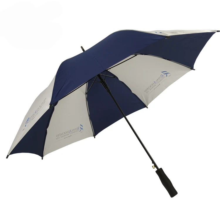
OEM ODM, настоящее изобретение, персонализированный прямой автоматический открытый пользовательский логотип, рекламный зонт для гольфа с логотипом для отелей
842,39-938,53 ₽