Изготовление файла Bom Gerber Бесплатная цитата изготовленный на заказ прототип Fr4 толщиной 1 унция стандартная печатная плата из тяжелой меди
- Категория: PCB & PCBA >>>
- Поставщик: Jinhua Technology (shenzhen) Co. Ltd.
Сохранить в закладки 1600549199557:
Описание и отзывы
Характеристики
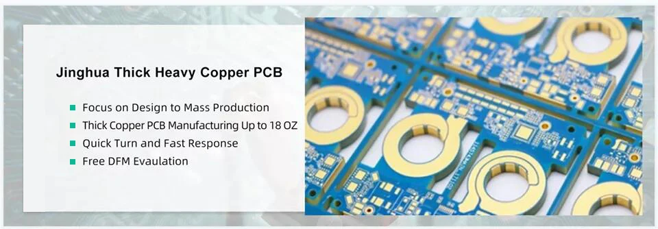
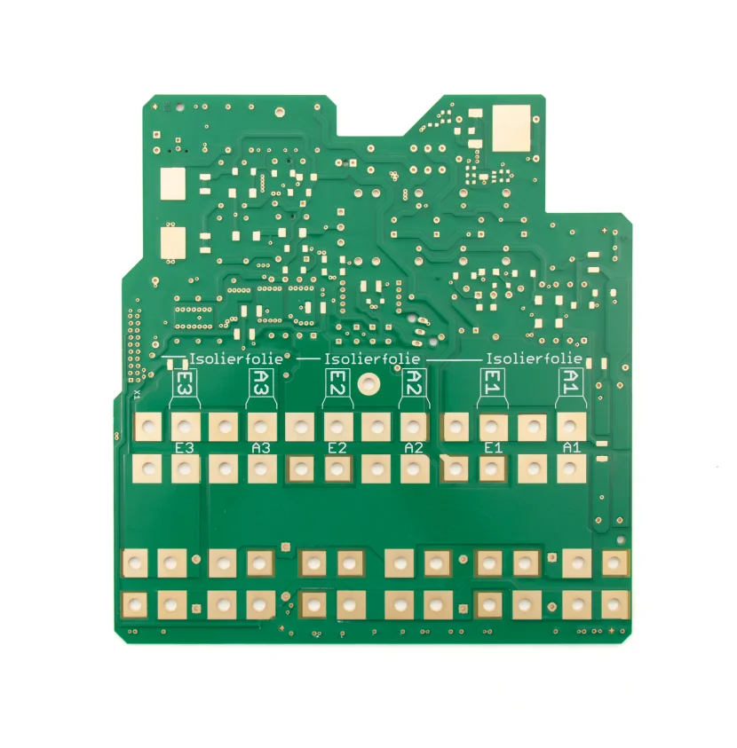
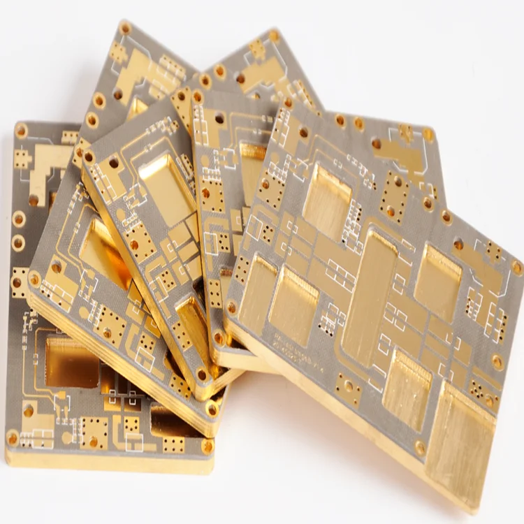
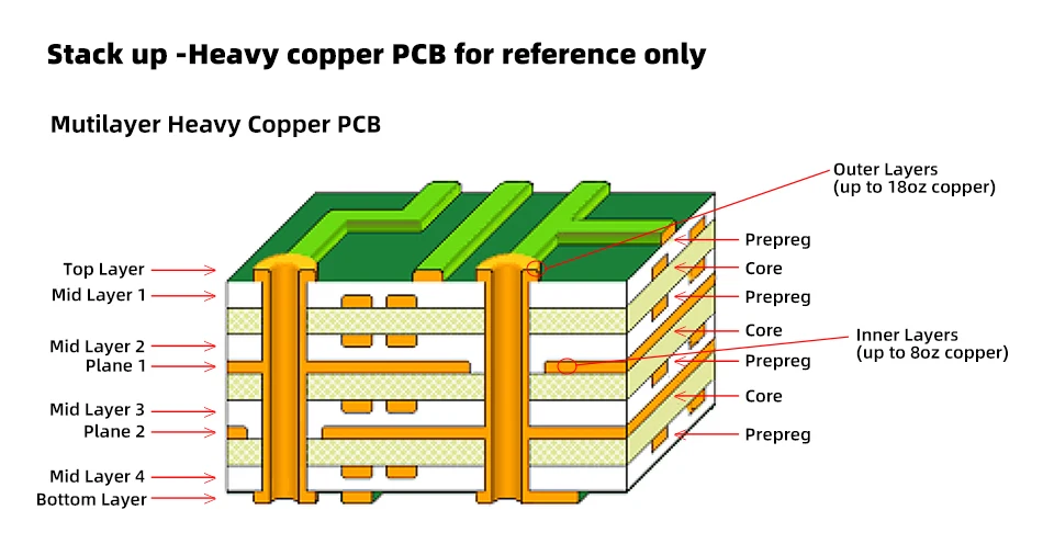
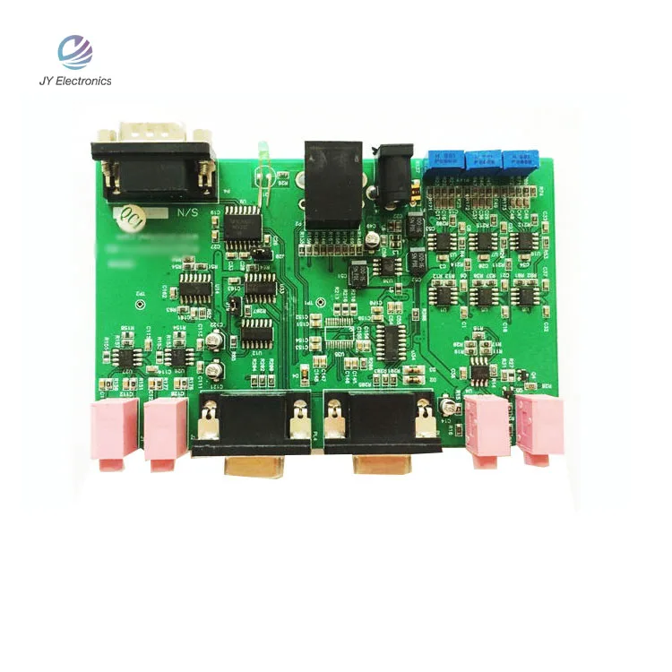
Heavy copper PCB is a circuit board with a copper thickness that is ≥ 3oz per sq. ft in its outer and inner layers. What makes a circuit board classified as a heavy copper PCB is its thicker plating. During the production of heavy copper PCB, copper thickness is enhanced through plated holes and sidewalls.
Why Choose Thick Copper PCB for your Applications
.Can withstand frequent exposure to excessive current
.High tolerance capacity
.Excellent endurance to thermal strains
.Better current conductivity
.Can survive repeated thermal cycling
.Smaller PCB sizes due to copper layers
.Reduced failure rates
.Increased connector site strength
.Lower production costs
.Excellent mechanical strength at connector sites and in PTH holes.
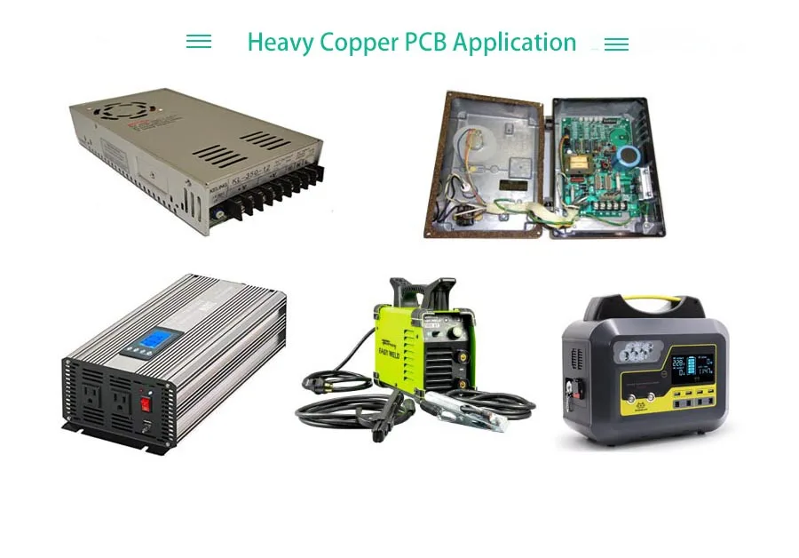
Applications of Thick Copper PCB
Heavy Copper PCB offers some outstanding features that make it ideal for certain applications. Such as:
Rail traction systems, UPS systems, Solar power converters, Automotive industries,Nuckear power industries
Power line motors, Welding equipment, Military equipment, Safety and signal systems, Protection relays
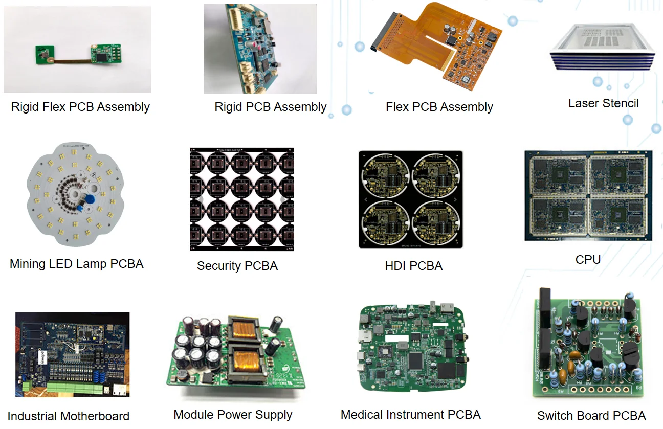
Related Products
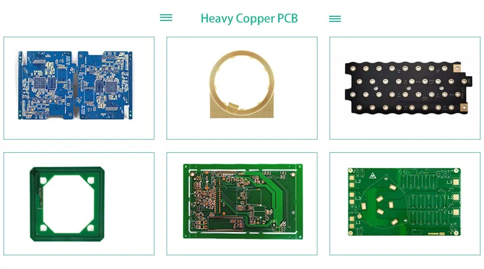
Product Description
| Process capability of thick copper PCB | ||
| Items | Content | Jinghua Capacity |
| 1 | Number of Layers | 2-24L |
| 2 | Materials | FR-4 Tg 140-170℃ |
| 3 | Finished Board Size | Min 6mm*6mm | Max 457*610mm |
| 4 | Board Thickness(Min-Max) | 0.5-6.0mm |
| 5 | Finished Thickness Tolerance | 10% |
| 6 | Copper Thickness(Min-Max) | 1oz - 18oz |
| 7 | Copper Plating Holes | 20µm ( 25µm ) |
| 8 | Solder Mask Color | Green, Blue, Red, Black, White, Purple, Yellow |
| 9 | Silkscreen Color | White, Yellow, Black |
| 10 | Surface Treatment | Immersion Gold, OSP, and HASL-LF |
| 11 | Build Time | 24H to 3 weeks |
| 12 | Standards | UL94V.0, IPC-6012, 6013, ISO-9001, ISO-14001 |
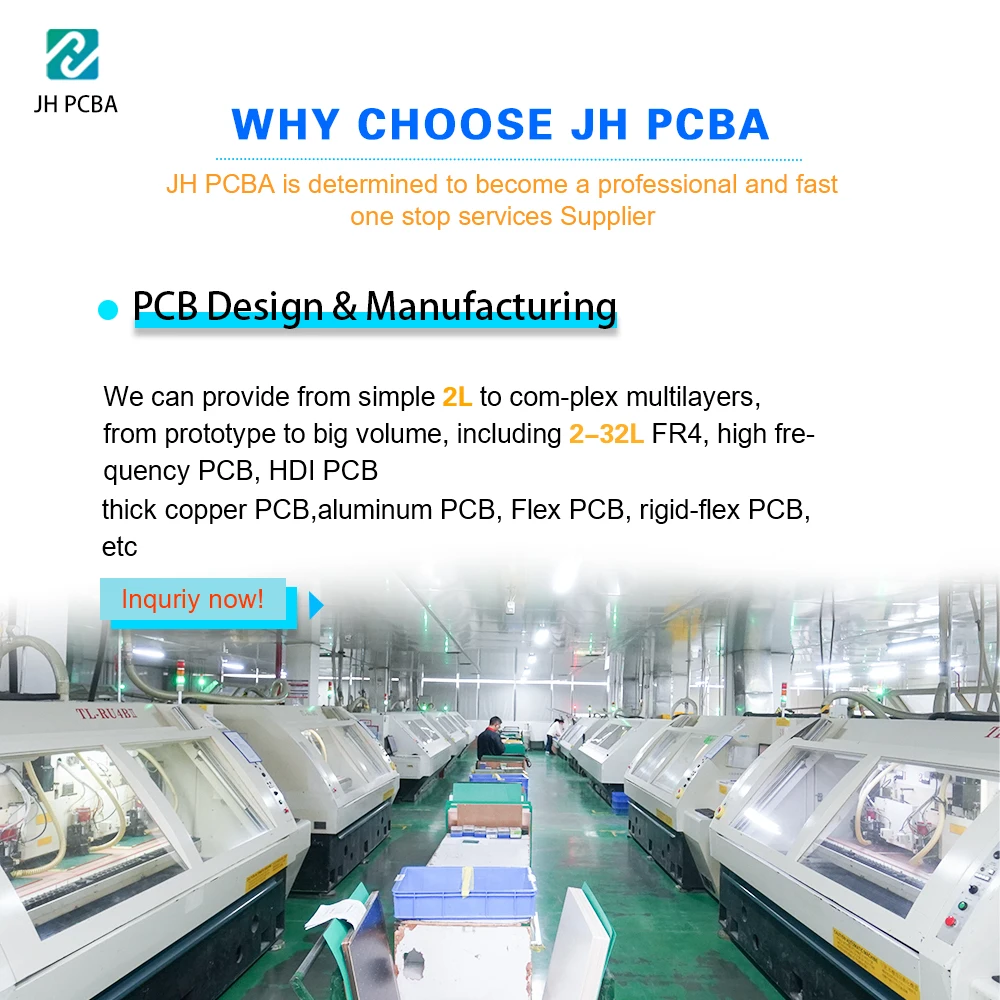
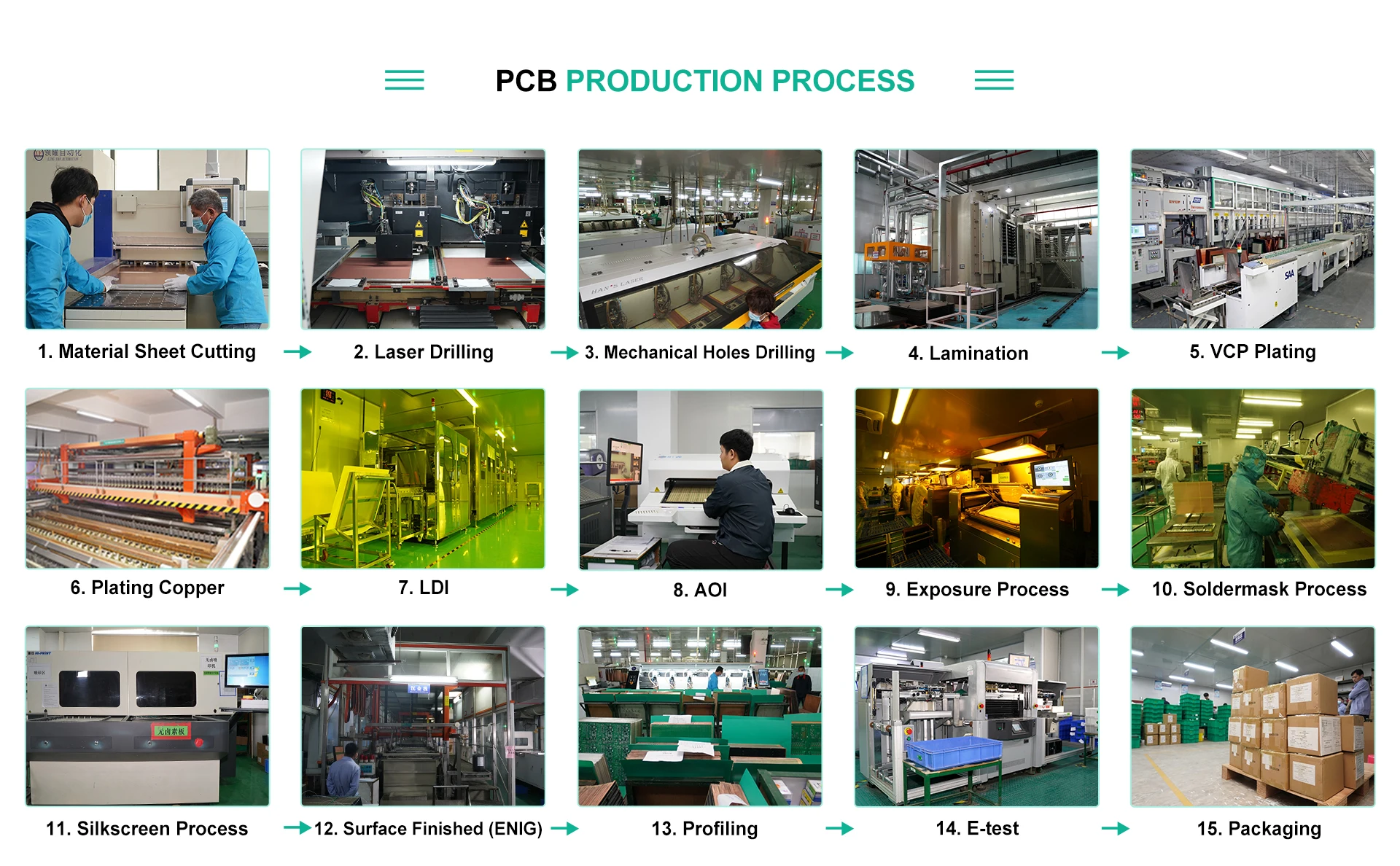
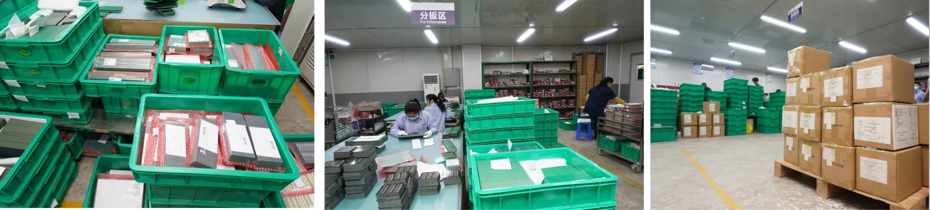
Production Process
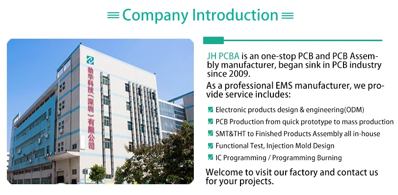
Company Information
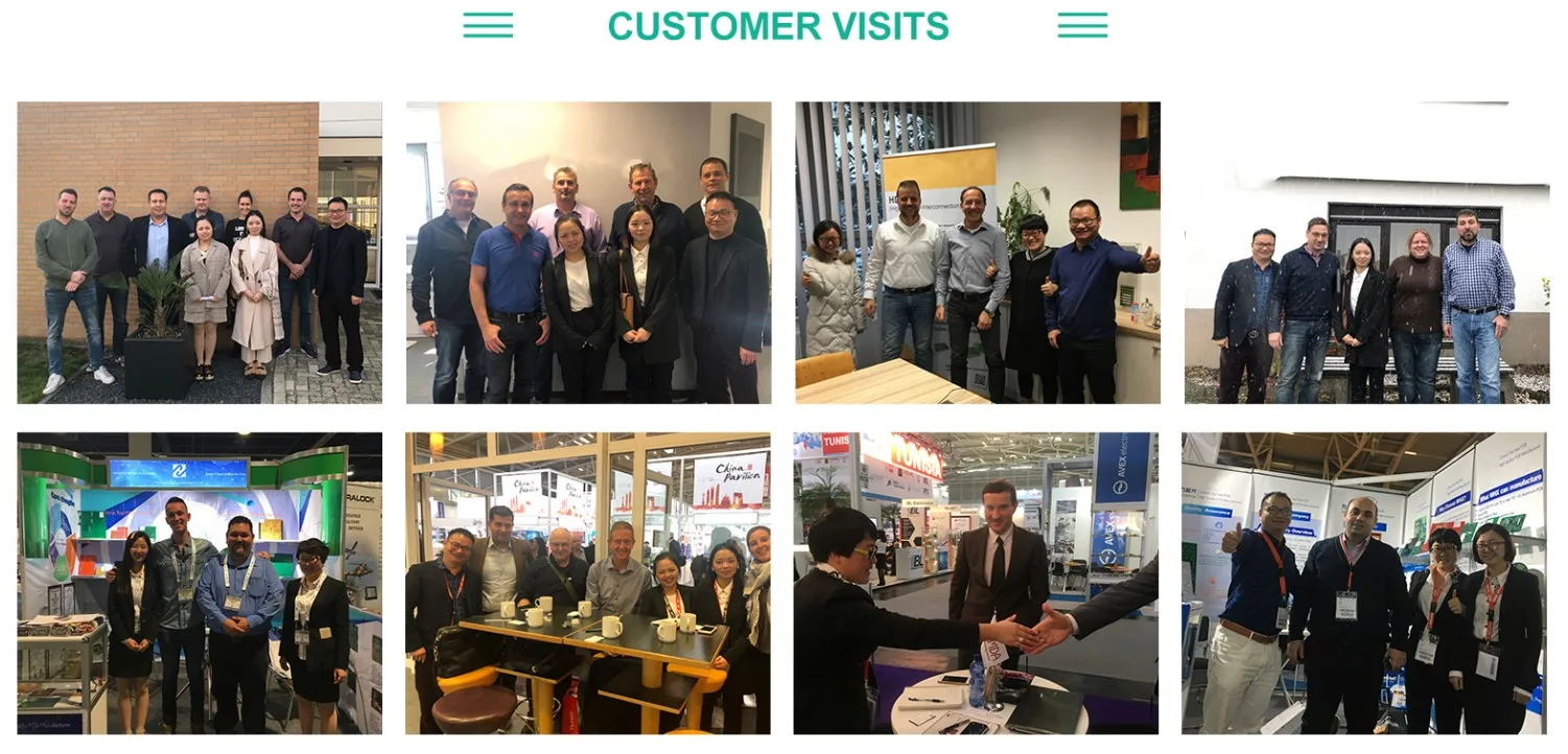
Exhibition
Packaging
FAQ
Q: Can a heavy copper PCB help reduce my product size?
A: Yes, Heavy Copper Boards can help reduce product size as it is possible to incorporate multiple copper weights on the same layer of circuity.
Q: What are the main advantages of a heavy copper PCB?
A: Increased current carrying capacity, increased endurance to thermal strain and increased mechanical strength at connector sites and in PTH holes.
Q: I need to put 55 Amps through my client. Can you advise on a Heavy Copper PCB design?
A: 55 Amps is not a problem. We can advise on all aspects of your Heavy Copper project.
Q: I need minimise package size, can I have a control section and a power section on a PCB?
A: By incorporating a multiple stage additive processing Heavy Copper boards allow for selected areas of a PCB to be plated to different copper weights. Typically used on the external layers of a PCB this process enables the control section and the power section to be on one panel reducing size and layer count.
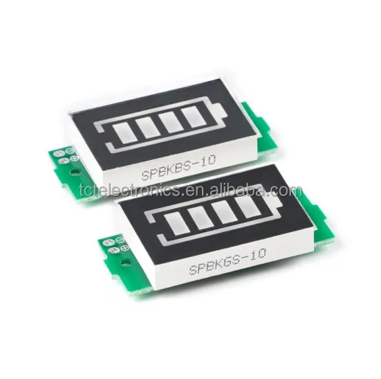
Похожие товары
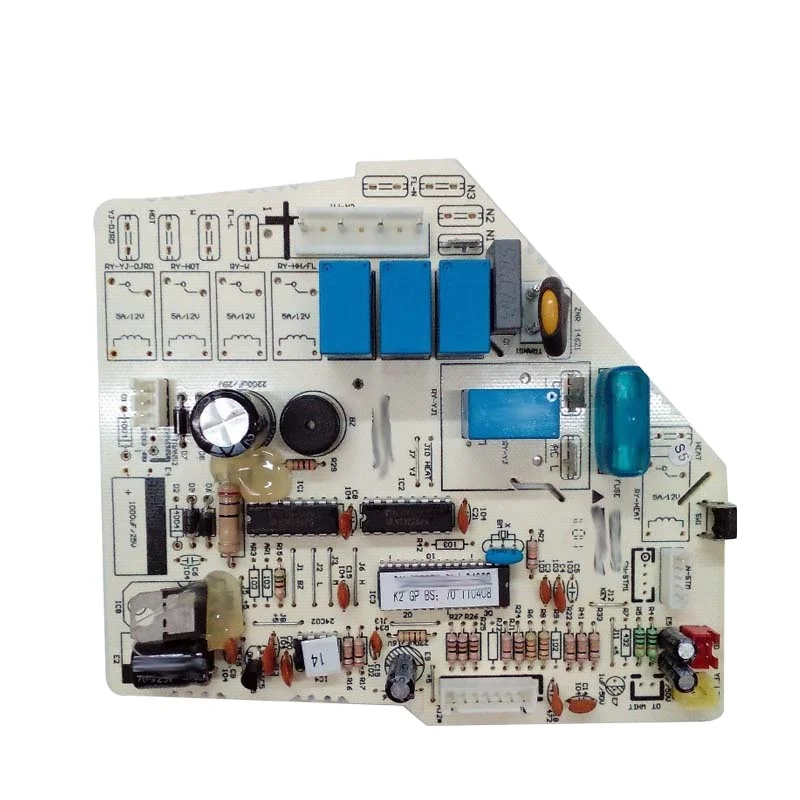
OEM высококачественные печатные платы для инвертора
0,40 $ - 0,50 $
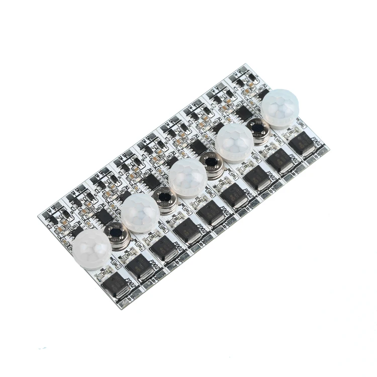
Ficlux PCBA 5 В 12 24 постоянного тока 10A PIR датчик обнаружения человеческого
0,99 $ - 2,00 $
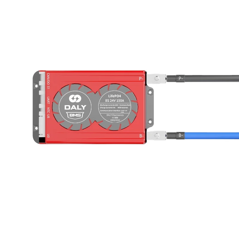
Запуск автомобиля Daly BMS LifePO4 4S/8S LTO 10S 100A/150A с функцией консервной установки для кабана парковочный кондиционер smart 12v
55,20 $ - 63,10 $
JINHUA многослойная печатная плата с потайным отверстием под заказ от
0,10 $ - 3,50 $
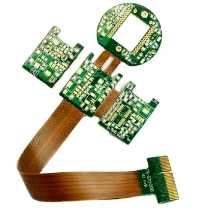
Изготовленная на заказ Многослойная Жесткая гибкая плата Pcb Производитель жестких гибких схем Заводская служба производства печатных
Высококачественное оборудование для клонирования печатных плат интегральная микросхема программное обеспечение трещин PCBA инженер по реверсу с предоставленными файлами Gerber
1,50 $ - 2,50 $
Печатная плата для домашнего кинотеатра Дронов печатная мобильного зарядного
0,70 $ - 1,00 $
Новые поступления
Новинки товаров от производителей по оптовым ценам
300 Вт безопасный для посудомоечной машины 5-скоростной турбо с крючками для теста, венчик, электрический ручной миксер
571,11-666,30 ₽
Медицинский портативный прибор для гемодиализа катетер и кровообращения диализа почек ухода за здоровьем
Многофункциональная роскошная водонепроницаемая палатка из брезента для кемпинга однокомнатная всесезонная с настраиваемым размером новый стиль рынка Ближнего Востока
45 688,76-56 159,10 ₽
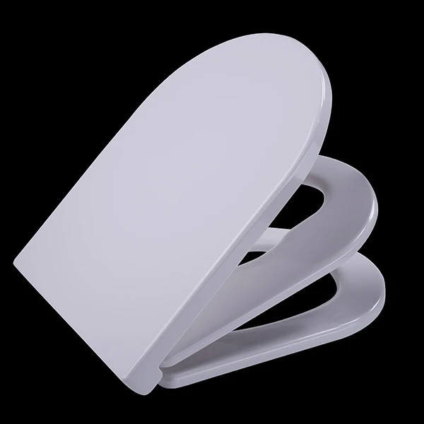
Санитарно-гигиеническое сиденье для
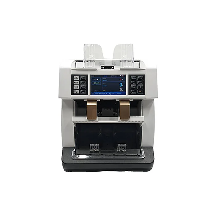
Счетчик купюр с низким уровнем шума на тонкопленочных транзисторах, автоматическое определение разных валют, 4,2 дюйма
50 448-52 351,70 ₽
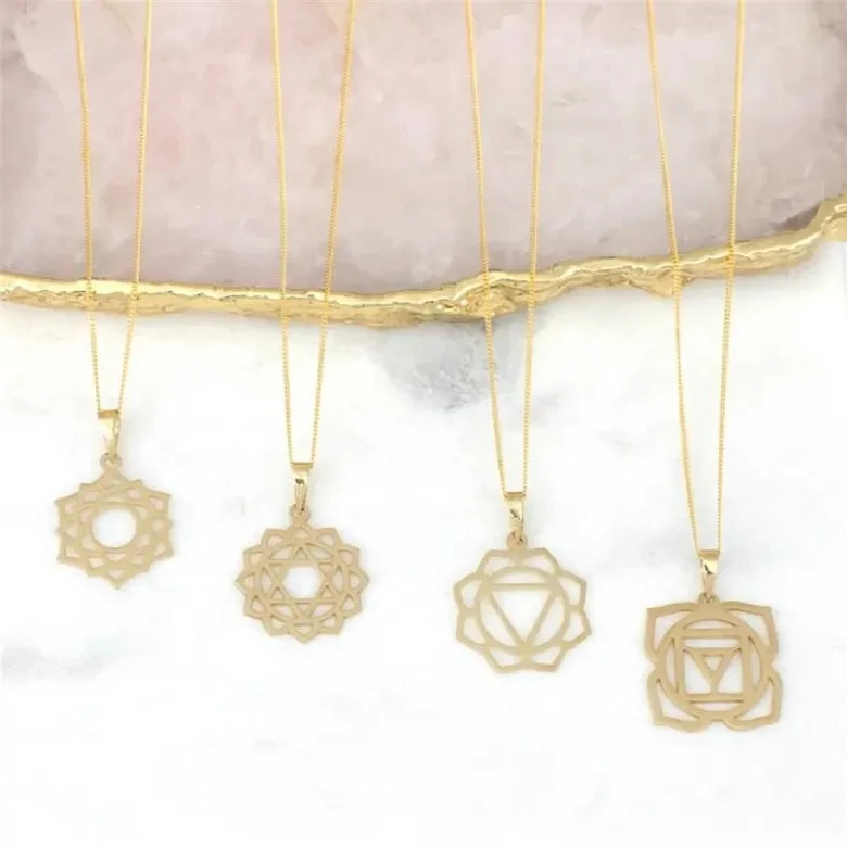
Ожерелье из нержавеющей стали изящное ожерелье с чакрами на заказ модное позолоченное ювелирное изделие водонепроницаемой подвеской без
121,84-217,03 ₽
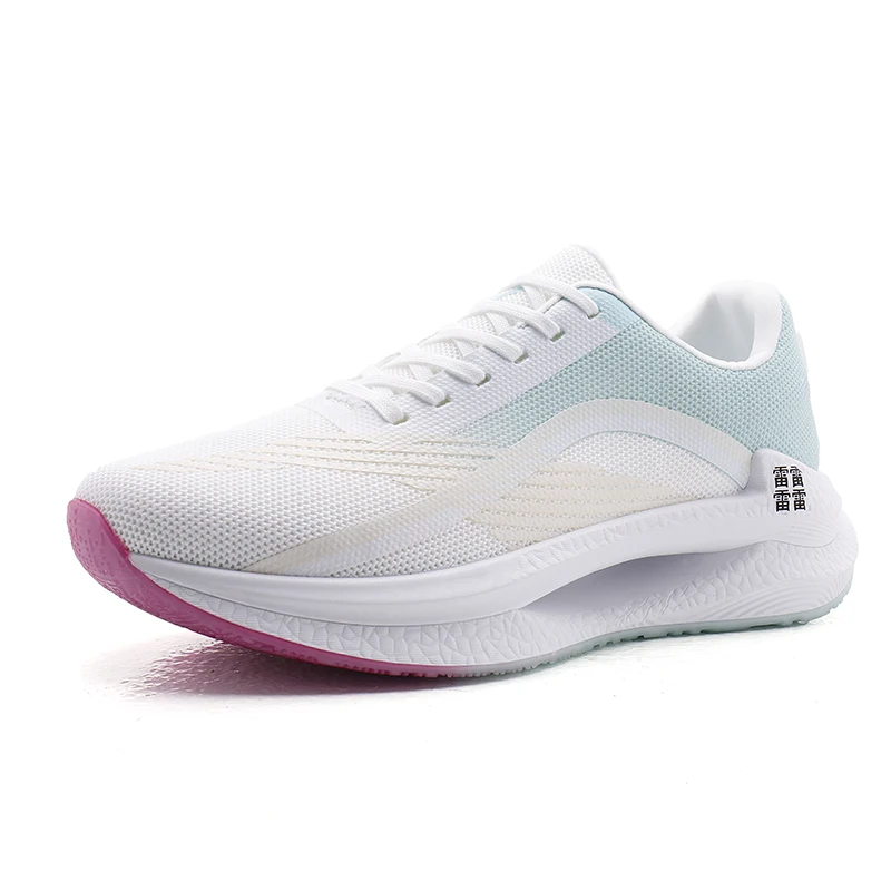
Мужские спортивные кроссовки с логотипом
856,67-999,45 ₽
OEM ODM, настоящее изобретение, персонализированный прямой автоматический открытый пользовательский логотип, рекламный зонт для гольфа с логотипом для отелей
842,39-938,53 ₽