


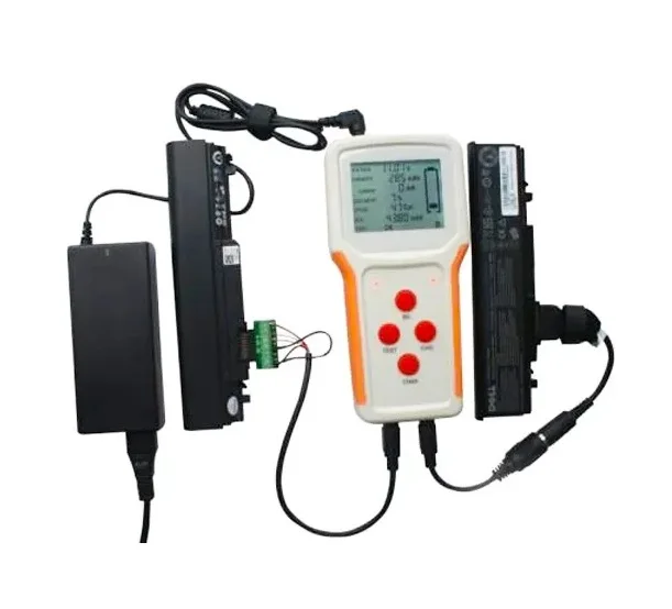
Универсальный тестер емкости аккумуляторов для ноутбуков RFNT2 профессиональный lifepo4 ремонта
23 283,68-32 480,74 ₽
Сохранить в закладки 1600643589349:
1. PCB/PCBA ODM & OEM Service
2.THREE SMT LInes, TWO DIP LINES and TWO Assembly Lines.
3. Five Engineers
4. ISO9001,RoHs,CE
PCB Capability | |
Layer count | 1-18 layers |
Material | fr4,Tg=135,150,170,180,210,cem-3,cem-1,al base,teflon,rogers,nelco |
Copper thickness | 1/2oz,1oz,2oz,3oz,4oz,5oz |
Board thickness | 8-236mil(0.2-6.0mm) |
Min.line width/space | 3/3 mil(75/75um) |
Min. drill size | 8 mil(0.2mm) |
Min. HDI laser drill size | 3 mil(0.067mm) |
Tolerance of hole size | 2 mil(0.05mm) |
PTH copper thickness | 1 mil(25 um) |
Solder mask color | Green,blue,yellow,white,black,red |
Peelable solder mask | Yes |
surface treating | HASL(ROHS), ENING,OSP,IMMERSION SILVER,IMMERSION TIN,flash gold |
Gold thickness | 2-30u" (0.05-0.76um) |
Blind hole/buried hole | Yes |
V-cut | Yes |
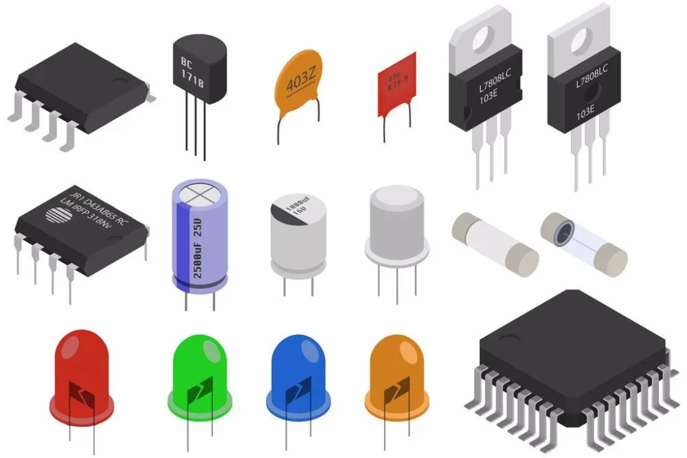
PCBA Capability | |
Technology | SMT, THT |
SMT capability | 2,000,000 points per day |
DIP capability | 300,000 points per day |
Experiences | QFP, BGA, μBGA, CBGA |
Process | Lead-free |
Programming | Yes |
Conformal coating | Yes |
Mobile Phone Charger PCBA ODM & OEM service
Ready mirror clock module with high accuracy
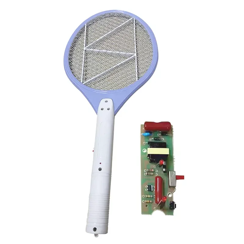
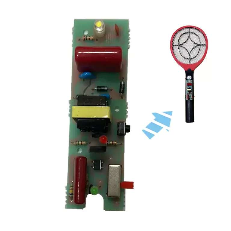
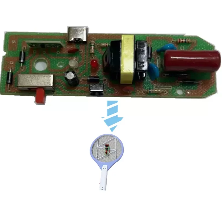
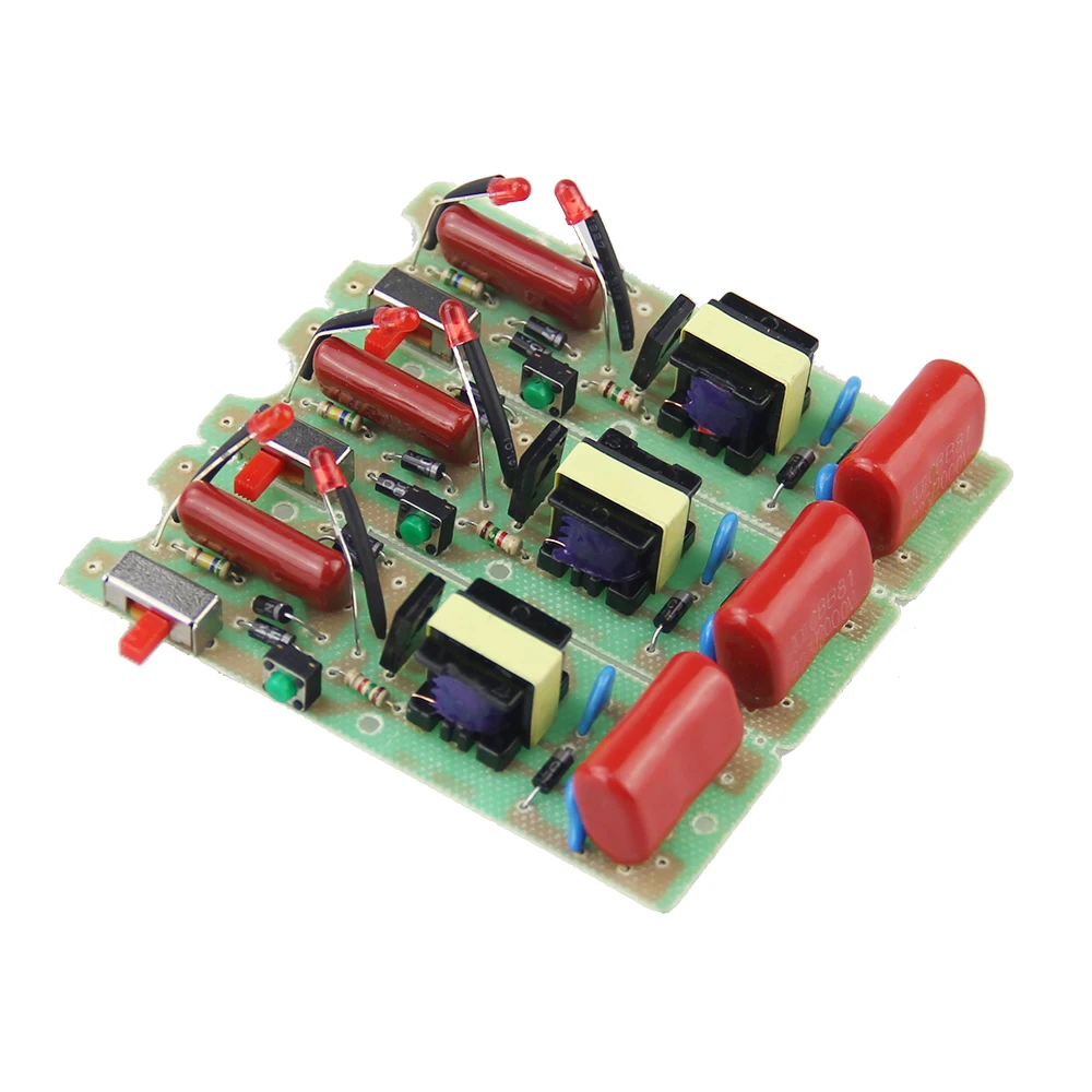
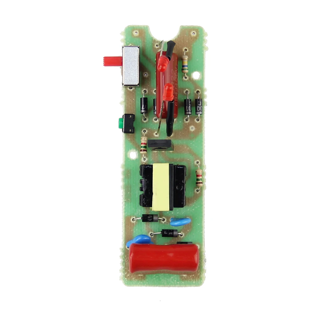
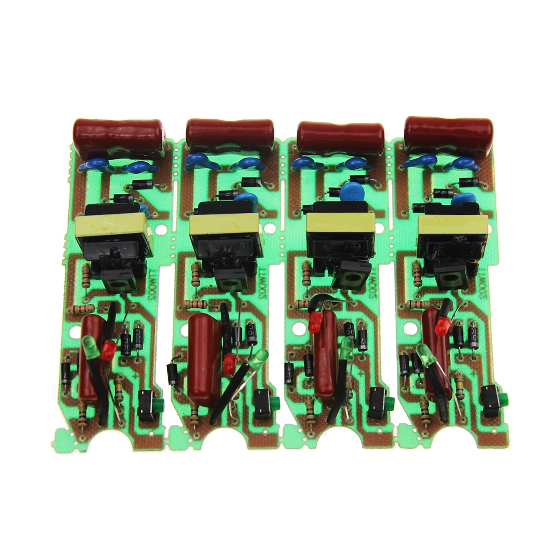
Ready Mosquito Killer Racket PCBA Mass Production and adjustment for your enclosures
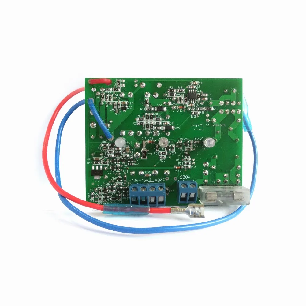
We provide PCB from 1 to 36 layers, with finished copper thickness 0.5-5 OZ, Min.Line/Track Width 3mil, Min.Line/Track Space 3mil, Min.Finished Diameter of PTH Hole 0.2mm.Surface Treatment HASL,ENIG,OSP etc.
We have rich experience in purchasing different kinds of electronic components for more than 20 years and established a long-term cooperation relationship with famous distributor for critical components.
We offer complete pcb assembly, can assemble PCB from 1 layer to 12 layers, components range from 0201,SIP,DIP to QFP,PLCC,BGA etc.
Based on PCBA and tooling capability, we offer complete product fabrication to finished electronic device.OEM and ODM orders are welcome.
R&D: According to customers requirements to make development
Test:AOI,X Ray, etc or specific test according to customers
Packing Details :Standard anti-static packaging
Delivery Details : 15-25 days after getting the deposit/full payment of order
A: Gerber file, BOM list and Quantity.
A: Generally it is 5-10 days for samples and 20-25 days for mass production.
A: Yes, Of course.
A: Payment<=5000USD, 100% in advance. Payment>=5000USD, 30% T/T in advance ,balance before shippment.
Новинки товаров от производителей по оптовым ценам