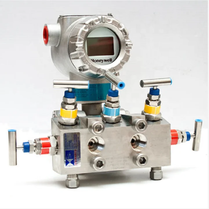
Сканер штрих-кода Honeywell Std810 Std820 Std830 Std870 Std800 Smartline передатчик перепада давления
460,00 $
Сохранить в закладки 1600763803695:
| Pin No. | Symbol | Pin Type | Description | ||||||||||||||||||||
|---|---|---|---|---|---|---|---|---|---|---|---|---|---|---|---|---|---|---|---|---|---|---|---|
| 1 | NC | - | No connection | ||||||||||||||||||||
| 2 | VSL | P | This is segment voltage (output low level) reference pin. When external VSL is not used, this pin should be left open. When external VSL is used, connect with resistor and diode to ground (details depend on application). | ||||||||||||||||||||
| 3 | VSS | P | Ground pin. It must be connected to external ground. | ||||||||||||||||||||
| 4 | REGVDD | I | Internal VDD regulator selection pin in 5V I/O application mode. When this pin is pulled HIGH, internal VDD regulator is enabled (5V I/O application). When this pin is pulled LOW, internal VDD regulator is disabled (Low voltage I/O application). | ||||||||||||||||||||
| 5 | SHLC | I | This pin is used to determine the Common output scanning direction. COM scan direction
Note (1) 0 is connected to VSS (2) 1 is connected to VDDIO | ||||||||||||||||||||
| 6 | SHLS | I | This pin is used to change the mapping between the display data column address and the Segment driver. SEG scan direction
Note (1) 0 is connected to VSS (2) 1 is connected to VDDIO | ||||||||||||||||||||
| 7 | VDD | P | Power supply for core logic operation. VDD can be supplied externally or regulated internally. In LV IO application (internal VDD is disabled), this is a power input pin. In 5V IO application (internal VDD is enabled), VDD is regulated internally from VDDIO. A capacitor should be connected between VDD and VSS under all circumstances. | ||||||||||||||||||||
| 8 | VDDIO | P | Low voltage power supply and power supply for interface logic level in both Low Voltage I/O and 5V I/O application. It should match with the MCU interface voltage level and must be connected to external source. | ||||||||||||||||||||
| 9 | BS0 | I | MCU bus interface selection pins. Select appropriate logic setting as described in the following table. BS2, BS1 and BS0 are pin select. Bus Interface selection
Note (1) 0 is connected to VSS (2) 1 is connected to VDDIO | ||||||||||||||||||||
| 10 | BS1 | ||||||||||||||||||||||
| 11 | BS2 | ||||||||||||||||||||||
| 12 | GPIO | I/O | It is a GPIO pin. Details refer to OLED command DCh. | ||||||||||||||||||||
| 13 | CS# | I | This pin is the chip select input connecting to the MCU. The chip is enabled for MCU communication only when CS# is pulled LOW (active LOW). In I2C mode, this pin must be connected to VSS. | ||||||||||||||||||||
| 14 | RES# | I | This pin is reset signal input. When the pin is pulled LOW, initialization of the chip is executed. Keep this pin pull HIGH during normal operation. | ||||||||||||||||||||
| 15 | D/C# | I | This pin is Data/Command control pin connecting to the MCU. When the pin is pulled HIGH, the data at D[7:0] will be interpreted as data. When the pin is pulled LOW, the data at D[7:0] will be transferred to a command register. In I2C mode, this pin acts as SA0 for slave address selection. When serial interface is selected, this pin must be connected to VSS. | ||||||||||||||||||||
| 16 | R/W#(WR#) | I | This pin is read / write control input pin connecting to the MCU interface. When 6800 interface mode is selected, this pin will be used as Read/Write (R/W#) selection input. Read mode will be carried out when this pin is pulled HIGH and write mode when LOW. When 8080 interface mode is selected, this pin will be the Write (WR#) input. Data write operation is initiated when this pin is pulled LOW and the chip is selected. When serial or I2C interface is selected, this pin must be connected to VSS. | ||||||||||||||||||||
| 17 | E(RD#) | I | This pin is MCU interface input. When 6800 interface mode is selected, this pin will be used as the Enable (E) signal. Read/write operation is initiated when this pin is pulled HIGH and the chip is selected. When 8080 interface mode is selected, this pin receives the Read (RD#) signal. Read operation is initiated when this pin is pulled LOW and the chip is selected. When serial or I2C interface is selected, this pin must be connected to VSS. | ||||||||||||||||||||
| 18 | D0 | I/O | These pins are bi-directional data bus connecting to the MCU data bus. Unused pins are recommended to tie LOW. When serial interface mode is selected, D0 will be the serial clock input: SCLK; D1 will be the serial data input: SID and D2 will be the serial data output: SOD. When I2C mode is selected, D2, D1 should be tied together and serve as SDAout, SDAin in application and D0 is the serial clock input, SCL. | ||||||||||||||||||||
| 19 | D1 | ||||||||||||||||||||||
| 20 | D2 | ||||||||||||||||||||||
| 21 | D3 | ||||||||||||||||||||||
| 22 | D4 | ||||||||||||||||||||||
| 23 | D5 | ||||||||||||||||||||||
| 24 | D6 | ||||||||||||||||||||||
| 25 | D7 | ||||||||||||||||||||||
| 26 | IREF | I | This pin is the segment output current reference pin. IREF is supplied externally. A resistor should be connected between this pin and VSS to maintain current of around 15uA. | ||||||||||||||||||||
| 27 | ROM0 | I | These pins are used to select Character ROM; select appropriate logic setting as described in the following table. ROM1 and ROM0 are pin select as shown in below table: Character ROM selection
Note (1) 0 is connected to VSS (2) 1 is connected to VDDIO | ||||||||||||||||||||
| 28 | ROM1 | ||||||||||||||||||||||
| 29 | OPR0 | I | This pin is used to select the character number of character generator. Character RAM selection
Note (1) 0 is connected to VSS (2) 1 is connected to VDDIO | ||||||||||||||||||||
| 30 | OPR1 | ||||||||||||||||||||||
| 31 | VCOMH | P | COM signal deselected voltage level. A capacitor should be connected between this pin and VSS. No external power supply is allowed to connect to this pin. | ||||||||||||||||||||
| 32 | VCC | P | Power supply for panel driving voltage. This is also the most positive power voltage supply pin. It is supplied by external high voltage source. | ||||||||||||||||||||
| 33 | NC | - | No connection |
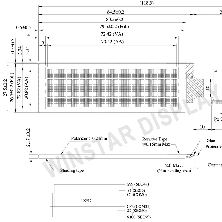
| Item | Dimension | Unit |
|---|---|---|
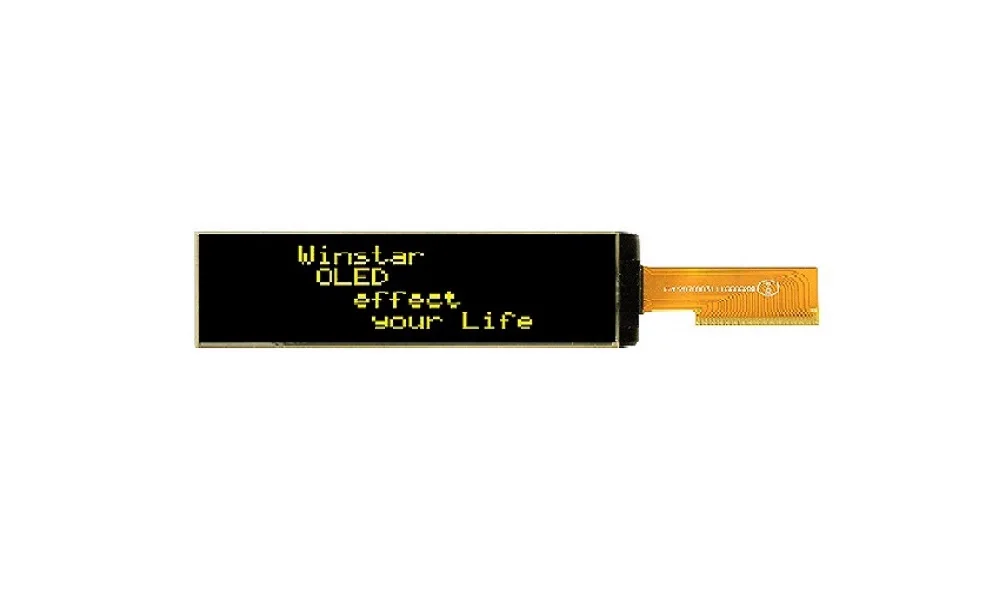
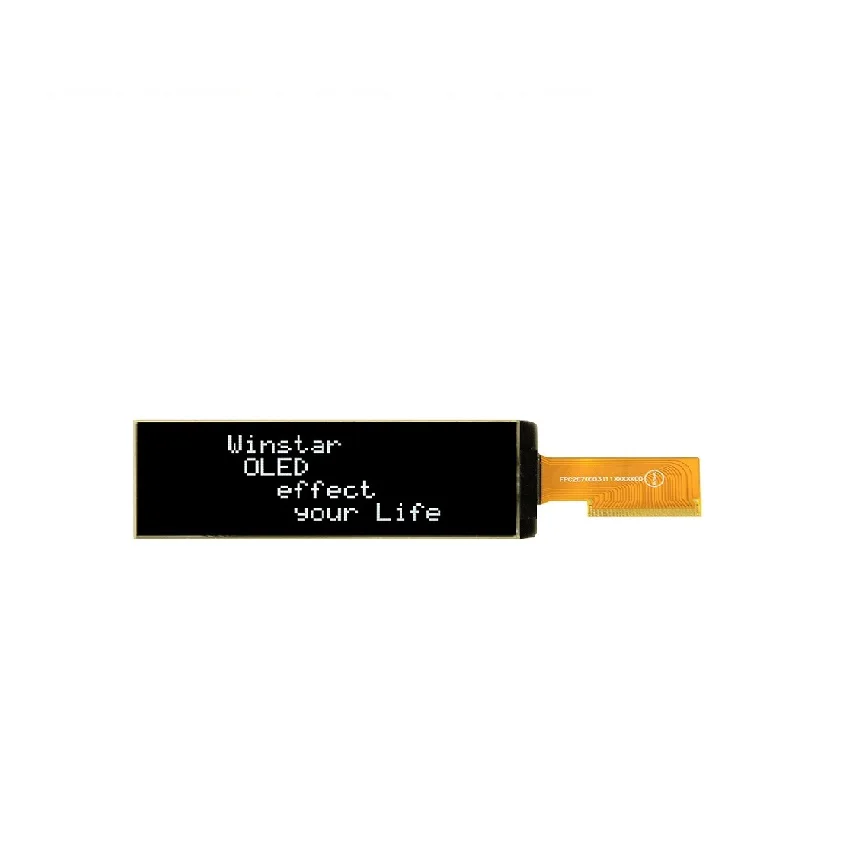
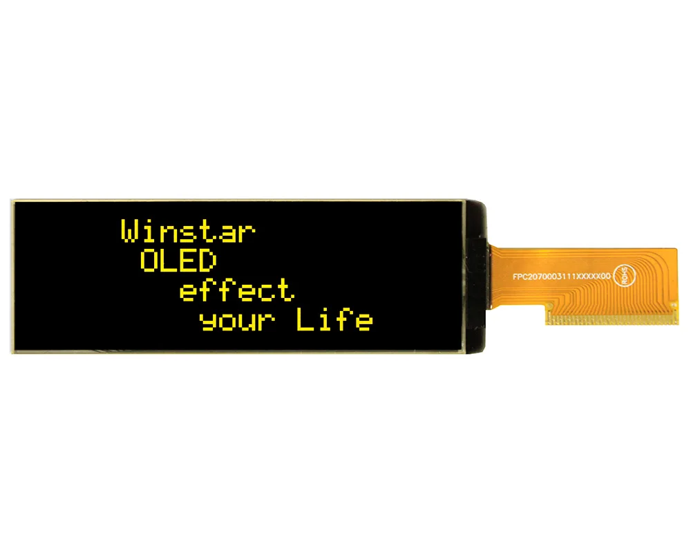
| Number of Characters | 20 characters x 4 Lines | - |
| Module dimension | 84.5 x 27.5 x 2.17 | mm |
| View area | 72.42 x 22.82 | mm |
| Active area | 70.42 x 20.82 | mm |
| Dot size | 0.57 x 0.57 | mm |
| Dot pitch | 0.60 x 0.60 | mm |
| Character size | 2.97 x 4.77 | mm |
| Character pitch | 3.55 x 5.35 | mm |
| LCD type | OLED , Monochrome | |
| Duty | 1/32 | |
| IC | SSD1311 | |
| Interface | 6800,8080,SPI,I2C | |
| Size | 2.89 inch | |


Новинки товаров от производителей по оптовым ценам