Морден животное слон и Жираф и живопись на холсте бабочка по номерам DIY цифровая картина маслом украшение для дома
2,50 $ - 2,88 $
Сохранить в закладки 60299204698:
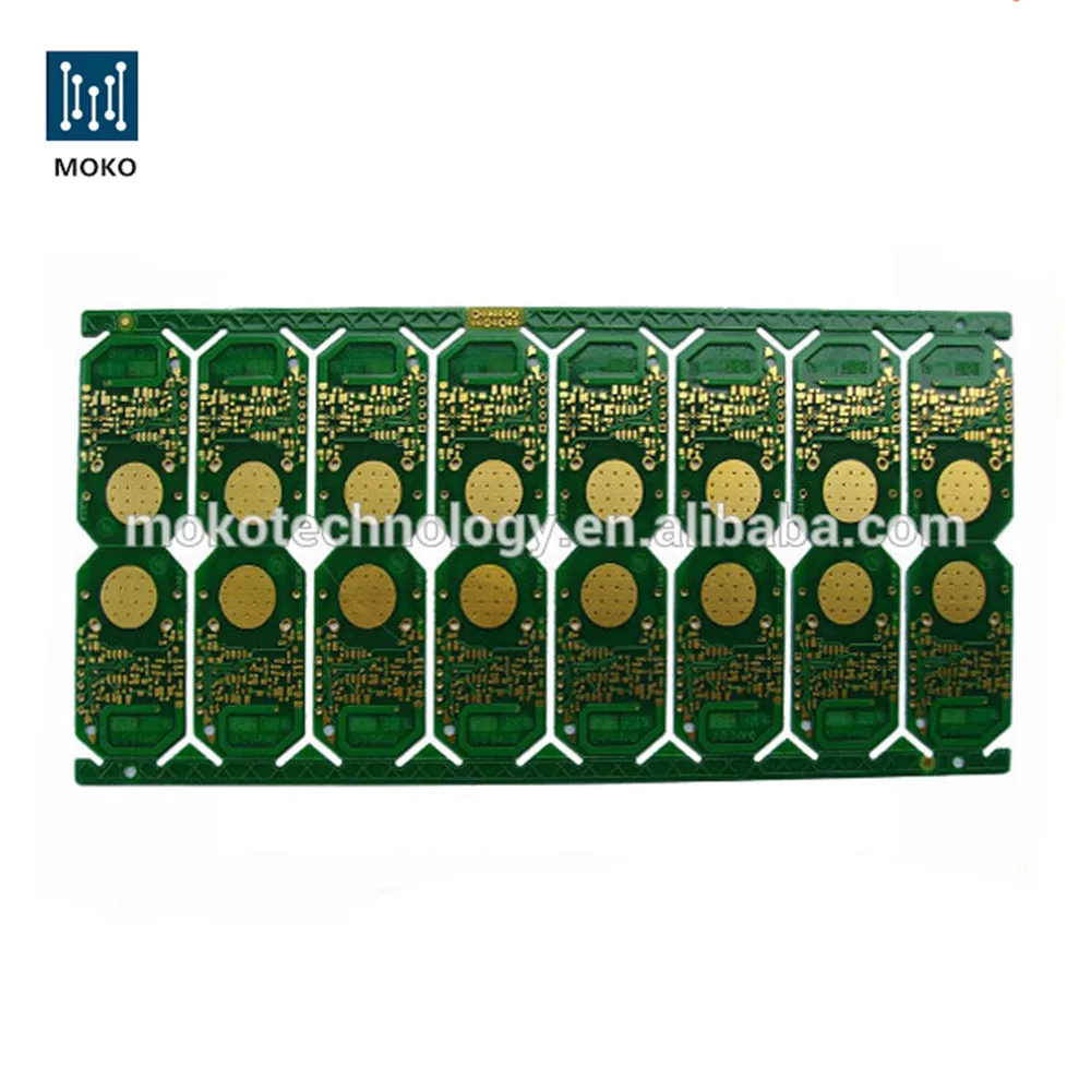
1. Single-Sided/ Double-Sided/ Multilayer OEM&ODM Electronic PCB Board.
2. HASL Surface Finishing Technology, Lead Free.
3. 100% Functional Tested.
4. UL,RoHS, SGS, ISO9001, ISO14001 Certificated.
5. 2 Years Warranty, We Protect Your Legal Interest Even We Are In Different Countries.
Here is the best choice for you, Single-Sided/ Double-Sided/ Multilayer FR-4 PCB Board with HASL surface finishing technology, We also make particular specification PCB/PCBA as you want if you send the Gerber file.
Your Trust Makes It A Great Honor For Our Team To Serve For Your Interest! We Take Your Opinion Seriously.
One Piece Order Accepted. Contact Us FOR MORE INFORMATION NOW!(Click to Visit Our Frontpage)


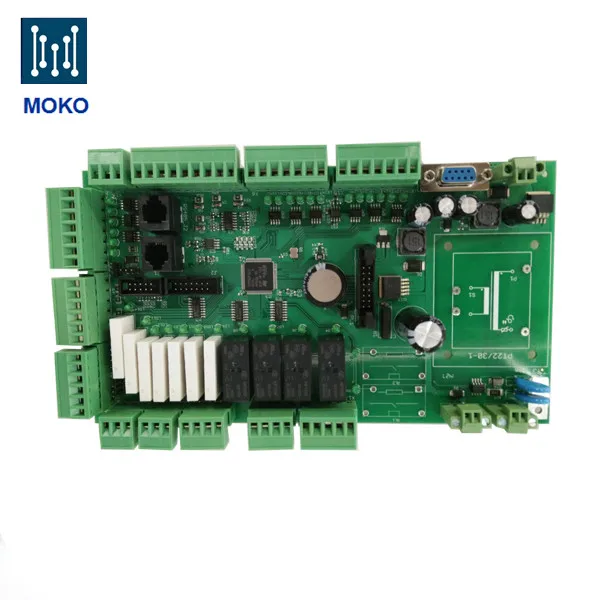
Founded in the year 2001,located in Shenzhen, as a professional OEM/ODM Manufacturer, MOKO is born to produce high quality product,provide the best engineer service,serve for our customers' core interests.We could provide one-stop pcb assembly service,we also offer:
- Contract Manufacturing
- Engineering Services
- PCB Design & Assembly
- Component Procurement & Material Management
- Product Design
- Fast Track Prototyping
- Cable and Wire Assemblies
- Plastics and Molds
- Function Testing Service
MOKO have adapted and developed our capabilities and skill set to meet every customer's requirement, from the manufacture of an appointed item to the whole engineering management. We are experienced in pcb fabrication, components sourcing and providing pcb engineering service.
Detailed Specification of PCB Manufacturing
| 1 | Layer | 1-30 layer |
| 2 | Material | FR-4,CEM-1,CEM-3,Hight TG,FR4 Halogen Free,FR-1,FR-2,Aluminum |
| 3 | Board thickness | 0.2mm-7mm |
| 4 | Max.finished board side | 500mm*500mm |
| 5 | Min.drilled hole size | 0.25mm |
| 6 | Min.line width | 0.075mm(3mil) |
| 7 | Min.line spaceing | 0.075mm(3mil) |
| 8 | Surface finish/treatment | HALS/HALS lead free,Chemical tin,Chemical Gold,Immersion gold Inmersion Silver/Gold,OSP,Gold Plating |
| 9 | Copper thickness | 0.5-4.0oz |
| 10 | Solder mask color | green/black/white/red/blue/yellow |
| 11 | Inner packing | Vacuum packing,Plastic bag |
| 12 | Outer packing | Standard carton packing |
| 13 | Hole tolerance | PTH:±0.076,NTPH:±0.05 |
| 14 | Certificate | UL,ISO9001,ISO14001,ROHS,CQC |
| 15 | Profiling Punching | Routing,V-CUT,Beveling |
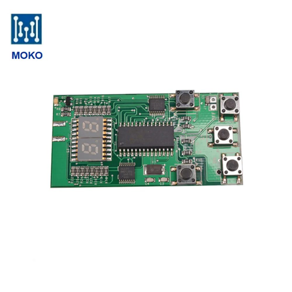
| 16 | Assembly Service | Providing OEM service to all sorts of printed circuit board assembly |
Technical requirement:
1) Professional Surface-mounting and Through-hole soldering Technology
2) Various sizes like 1206,0805,0603 components SMT technology
3) ICT(In Circuit Test),FCT(Functional Circuit Test) technology.
4) PCB Assembly With UL,CE,FCC,Rohs Approval
5) Nitrogen gas reflow soldering technology for SMT.
6) High Standard SMT&Solder Assembly Line
7) High density interconnected board placement technology capacity.
Quote requirement:
· Gerber file of the bare PCB board
· BOM (Bill of material) for assembly
· To short the lead time, please kindly advise us if there is any acceptable components substitution.
· Testing Guide & Test Fixtures if necessary
· Programming files & Programming tool if necessary
· Schematic if necessary
Orientronic PCB assembly Equipment:
· SMT Machine: SIEMENS SIPLACE D1/D2 / SIEMENS SIPLACE S20/F4
· Reflow Oven: FolunGwin FL-RX860
· Wave Soldering Machine: FolunGwin ADS300
· Automated Optical Inspection (AOI): Aleader ALD-H-350B
· Fully Automatic SMT Stencil Printer: FolunGwin Win-5
 PCB Leadtime:
| Single/double side | 4 layer | 6 layer | Above 8 layer | HDI | |
| Sample lead time(Normal) | 5-6 | 6-7 | 7-8 | 10-12 | 15-20 |
| Sample lead time(Fastest) | 48-72 hours | 5 | 6 | 6-7 | 12 |
| Mass production lead time(First batch) | 7-9 | 10-12 | 13-15 | 16 | 20 |
Shipping Methods
1.By DHL, UPS, FedEx, TNT using clients account.
2.By EMS (Usually for Russia Clients), but the price is high.
3.By sea for mass quantity according to customer's requirement.
4.By customer's Forwarder

1)RoHS SMT Processing:
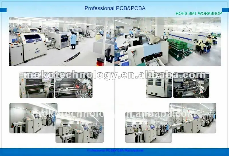
2)High Standard Through-Hole Components Soldering Workshop

3) Full Equipped Function Circuit Testing Room
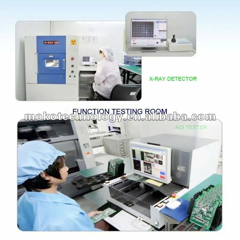
PCBA Products Showcase

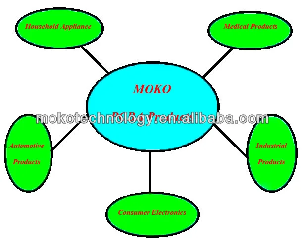
Products Application

Q:What's files do you use in the bare board fabrication?
A:Gerber RS-274X,274D,Eagle and AutoCAD's DXF,DWG
Q:What's files do you need in the PCBA projects?
A:Besides the pcb file, the PNP(Pick and Place) file and Components Position file are also needed.
Q: How can I know the processing about my PCB or PCBA order?
A: Each Customer will have a sale to contact with you. MOKO working hours:AM9:00-PM6:00(Beijing Time) from Monday to Friday. We will reply your email in 2 hours in our working time. And you also can contact with our sales's cell phone if urgent.
Q: Will our product be tested before shipment?
A: Yes, we could provide Function Circuit Testing if you provide us the testing methods.
Новинки товаров от производителей по оптовым ценам