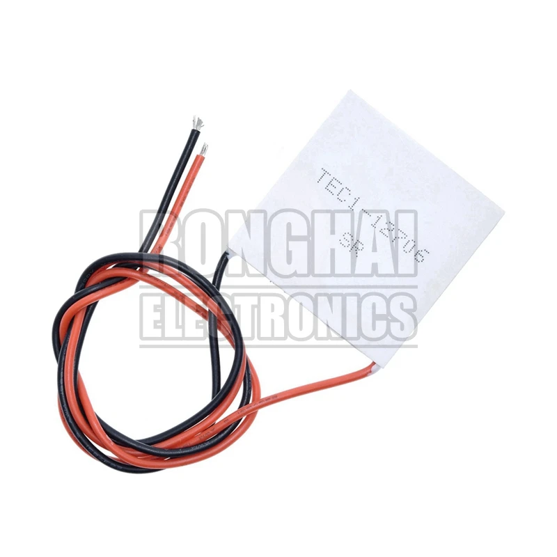
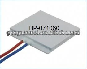
TEC1-12706 TEC Термоэлектрический охладитель Пельтье 40*40 мм
0,10 $ - 0,99 $


Сохранить в закладки 62226137072:
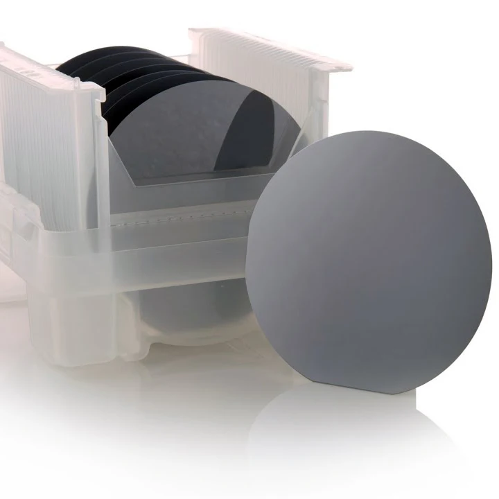
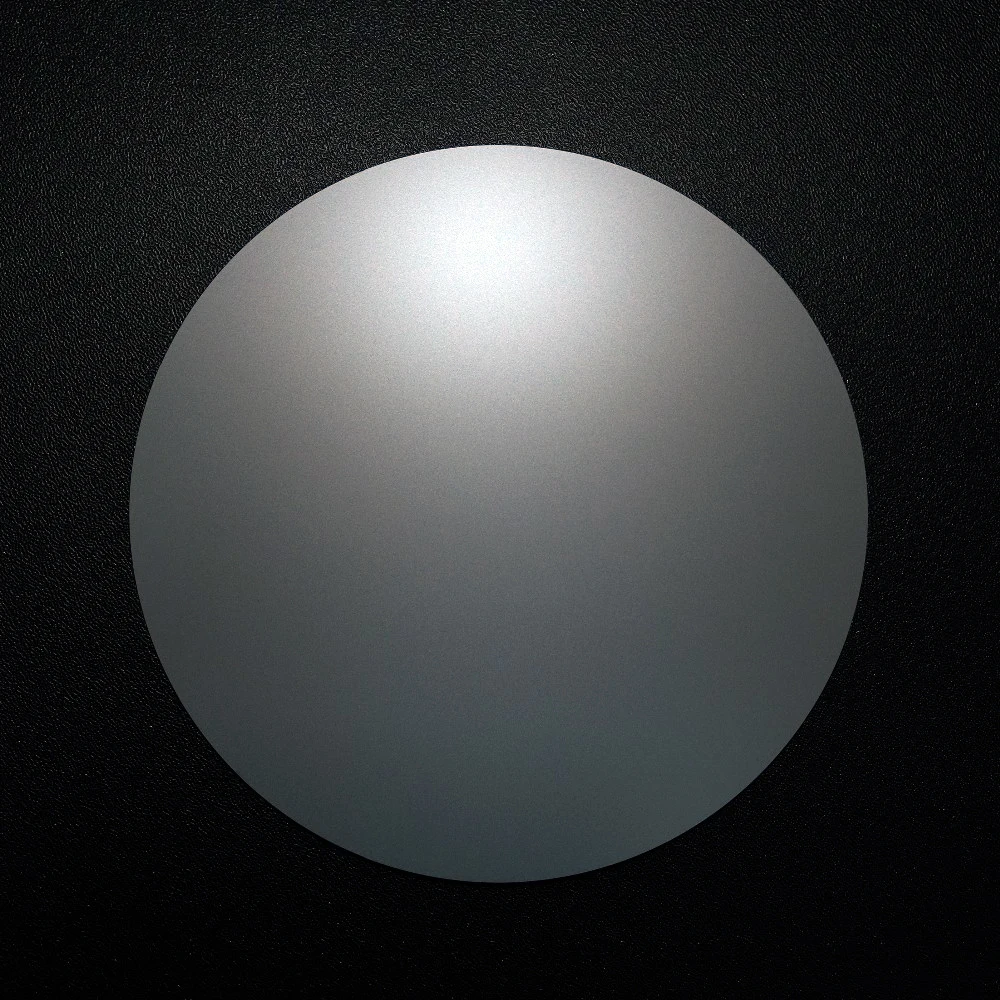
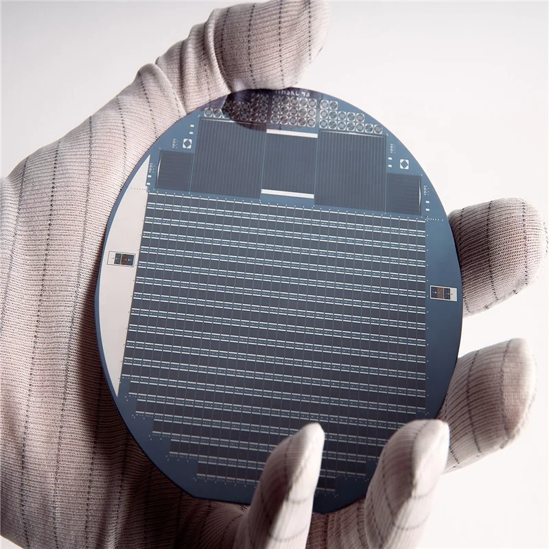
1. Diameter: 2’’ to 8’’inch
2. Surface quality: better than 40/20
3.Material: Silicon
4.Dimension Tolerance: +0.0/-0.1mm
5.Thickness Tolerance: ±0.1mm
6.Surface Quality: S1:20-10,S2:Fine Ground (As request)
We Know What You Need !
We understand your problems and can talk the language of your industry . Just talk to us , you can get benefits of our comprehensive fabrication know how , material features and problem-solving experiences .
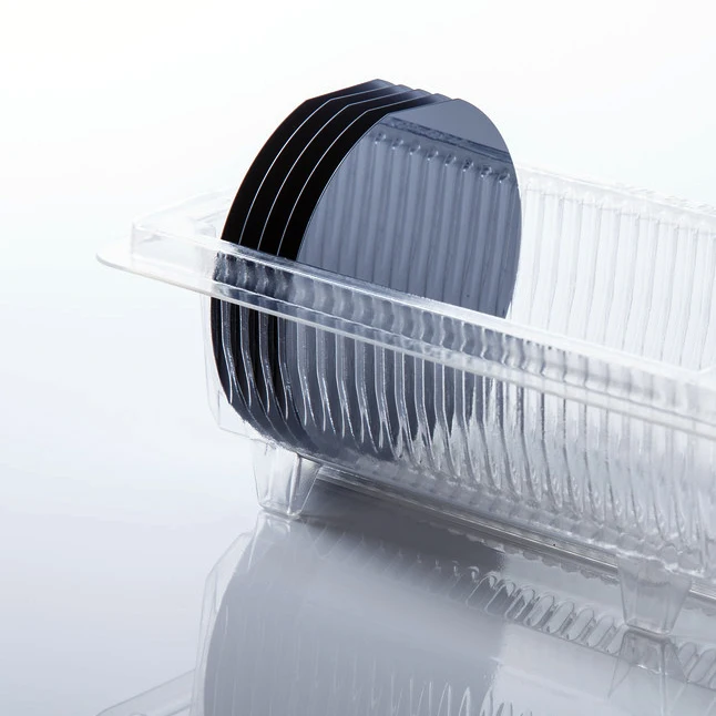
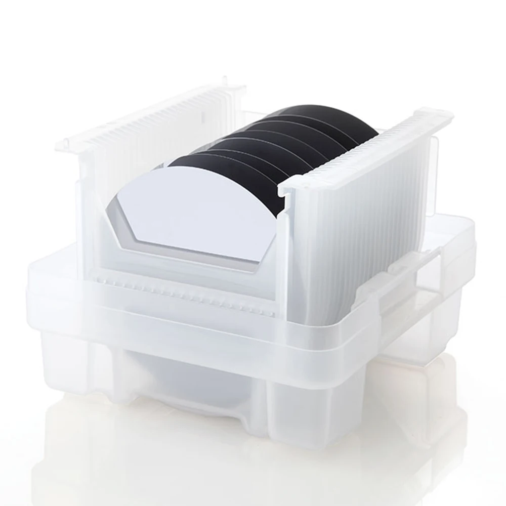
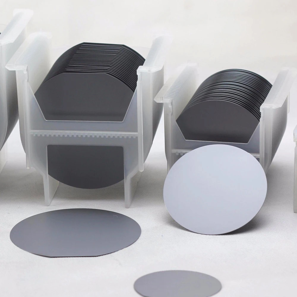
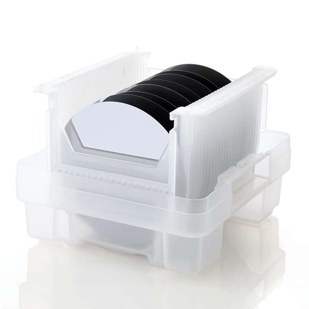
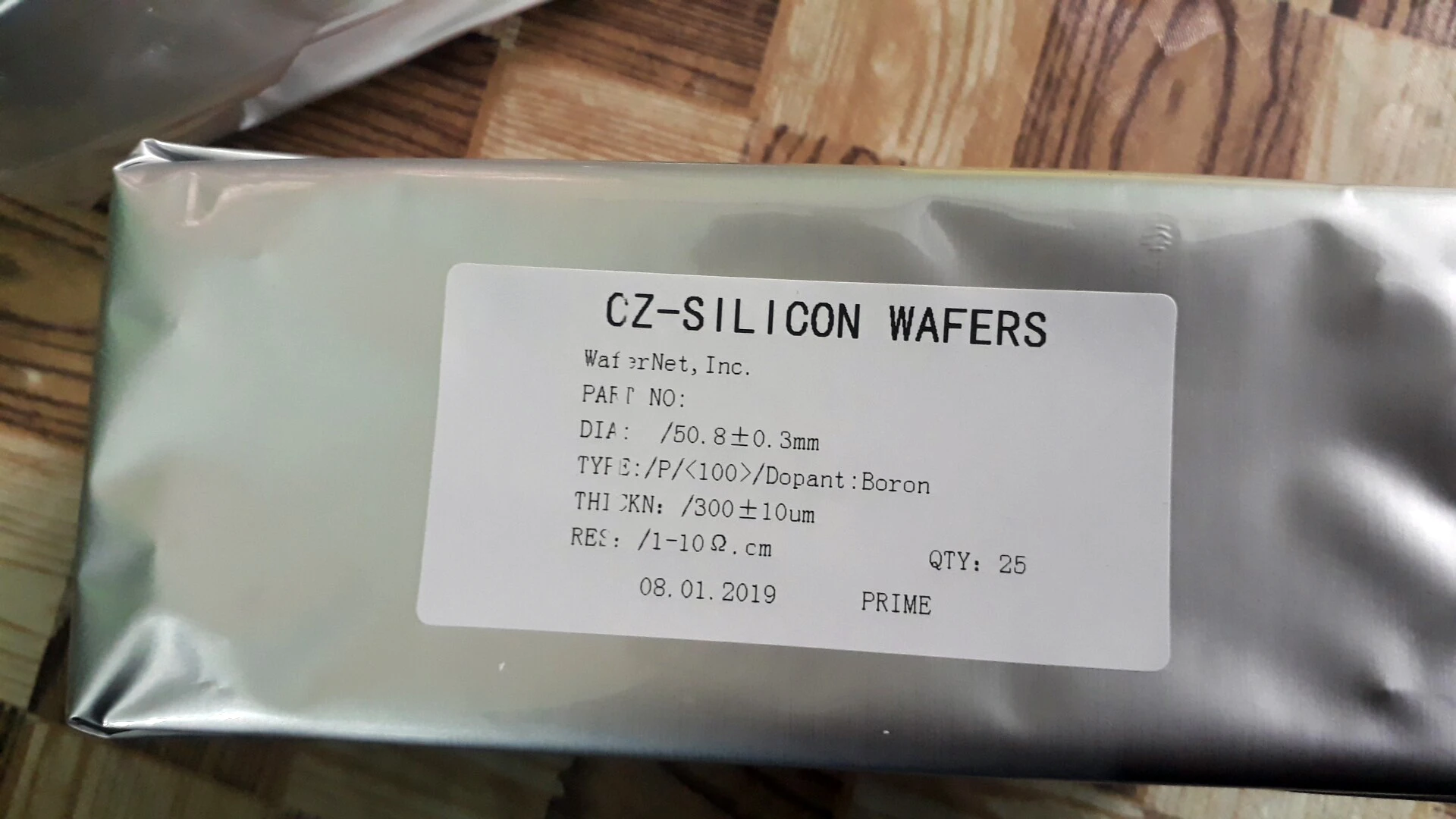
These 2" (50.8mm), 3" (76.2mm) and 4" (102mm) diameter silicon wafers can be used either as substrates for thin-film research or to make small silicon substrates by dicing the wafer into smaller pieces using a scriber. Wafers generally have flats or notches cut into one or more sides indicating the crystallographic plane and doping type. These silicon wafers are available as P-type (boron-doped) wafers which are cut with a primary flat. The wafers are 230 - 575µm thick polished on one side and do not have a silicon dioxide top coating. Each wafer is shipped in a wafer carrier.
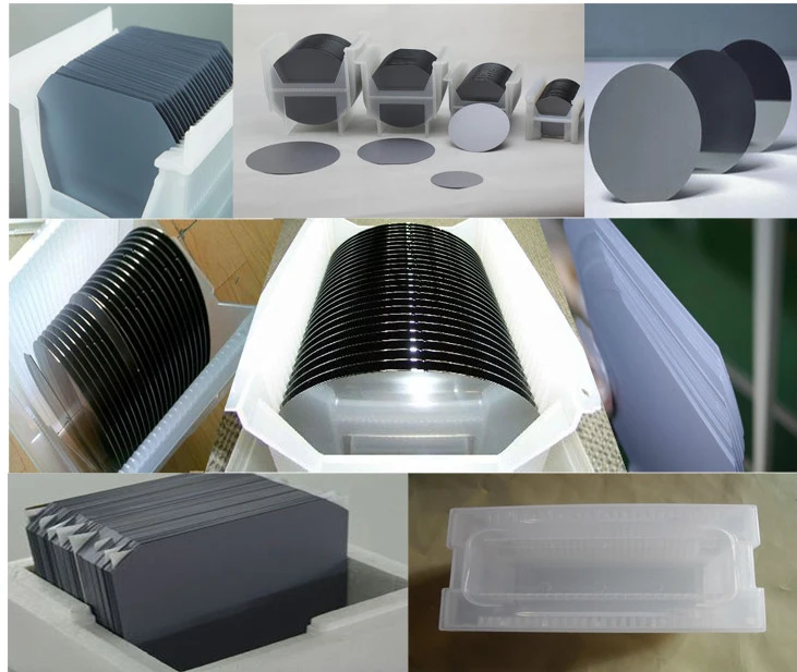
Silicon Wafer Available
| CZ or FZ Wafer | Prime Wafer |
| Intrinsic Wafer | Test Wafer |
| Heavily Doped Wafer | High Resistivity Wafer |
| Off Axis Orientation Wafer | Special Orientation Wafer |
| Ultra Flat Wafer | Ultra Thin Wafer |
| Ultra Thick Wafer | Double Sides Polished |
| Thermal Oxide Wafer | Epi Wafer |
Product Specification
| Growth | CZ / FZ |
| Diameter | Ø 2" / Ø 3" / Ø 4" / Ø 6" / Ø 8" / Ø 12" |
| Thickness | 275 um ~ 775 um |
| Orientation | <100> / <111> / <110> or others |
| Conductivity | P - type / N - type / intrinsic |
| Dopant | Boron / Phosphorous / Antimony / Arsenic |
| Resistivity | 0.001 ~ 10000 ohm-cm |
| Surface | One side polished / two sides polished |
| TTV | <= 10 um |
| Bow / Warp | <= 40 um |
| Grade | Prime / Test / Dummy grade |


Q: What's the way of shipping and cost?
A:(1) We accept DHL, Fedex, TNT, UPS, EMS etc.
(2) If you have your own express account, it's great.If not,we could help you ship them. Freight is USD30
Q: How to pay?
A: T/T, Paypal, Secure payment and Assurance payment on Alibaba.com and etc..
Q: What's your MOQ?
A: (1) For inventory, the MOQ is 25pcs/Box.
(2) For customized products, the MOQ is 50pcs.
Q: What's the delivery time?
A: (1) For the standard products
For inventory: the delivery is 5 workdays after you place the order.
For customized products: the delivery is 2 or 3 weeks after you place the order.
(2) For the special-shaped products, the delivery is 4 or 6 workweeks after you place the order.
Q: Do you have standard products?
A: Our standard products in stock.
Q: Can I customize the products based on my need?
A: Yes, we can customize the material, specifications and optical coating for your optical components based on your needs.
Q: Do you have inspection report for material?
A: We can supply ISO,CE etc for our products.
Q: How to ensure the safety of payment?
A: We are the gold supplier on alibaba.com and supports Alibaba Trade Assurance.

Please send us an inquiry, tell us your requirements, we will reply to you in 3hours.
↓↓↓
Новинки товаров от производителей по оптовым ценам