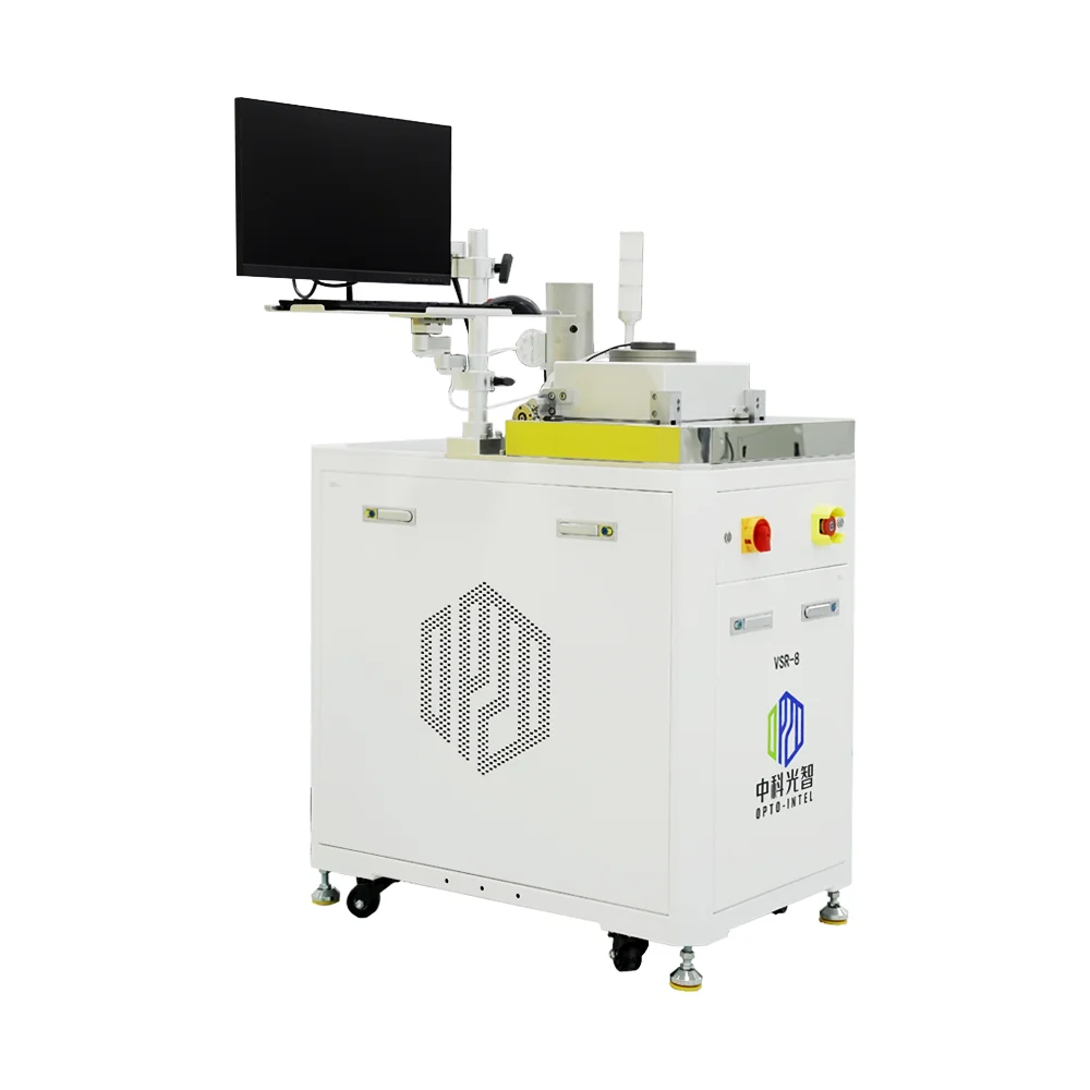
Длительное повторное использование бескислородной паяльной печи вакуумного опрокидывания для светодиодных уличных фонарей

Сохранить в закладки 1601190386629:
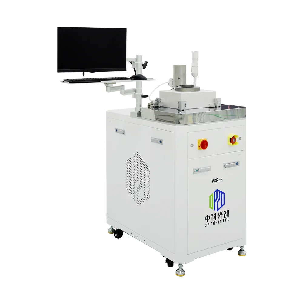
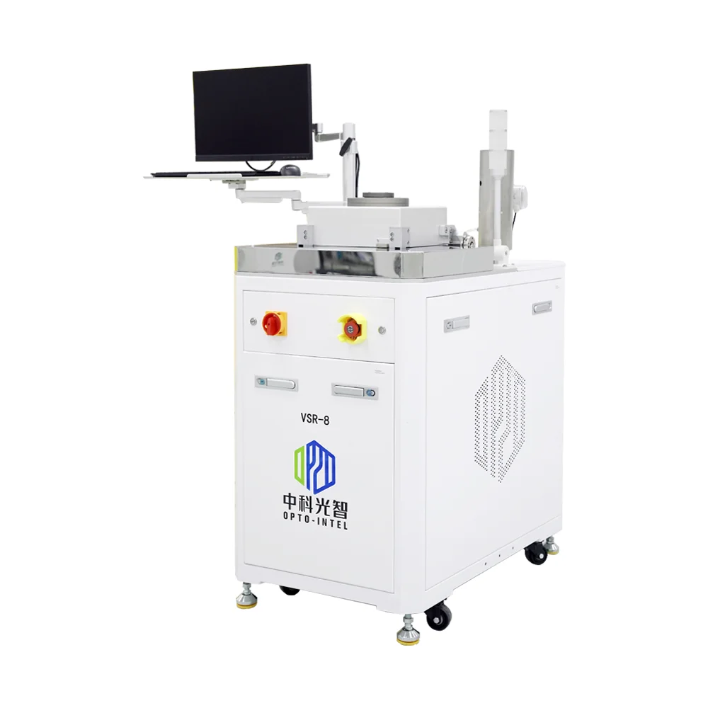
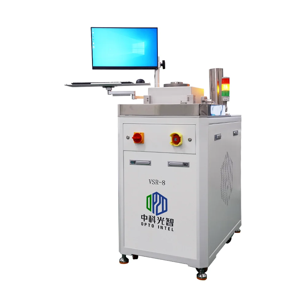
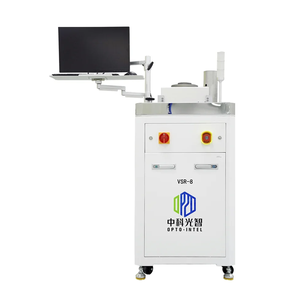
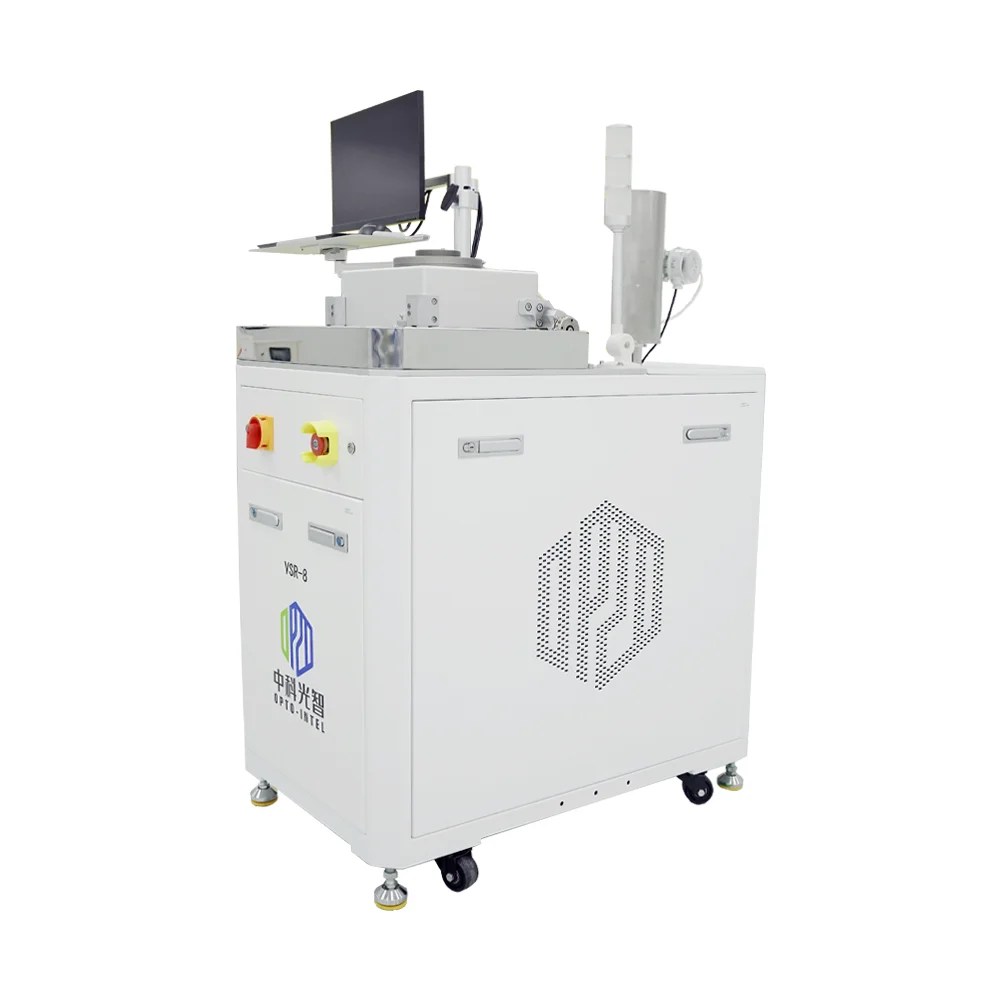
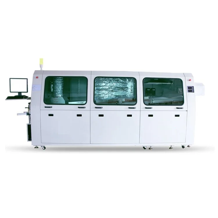

Цена:4 891 902,75 ₽ - 5 435 447,50 ₽*

Количество:

  • В избранное

Описание и отзывы

Характеристики


Product Description


Product Name
Vacuum Solder Reflow Oven
brand
opto-intel
Model number
VSR-8


Certificate


Packing&Shipping


Company Introduction


Opto-Intel Technologies Co., Ltd., headquartered in Chongqing, China, is a semiconductor assembly equipment manufacturer integrating R&D, manufacturing, and sales to provide professional services to the domestic and global markets. The company mainly focuses on the markets in semiconductors, optoelectronics, and advanced manufacturing, providing customers with process equipment and technical solutions.
With a core team with rich technical experience and outstanding innovation ability, the company has obtained more than 30 granted patents based on continuous technical development and has independently developed a number of featured products, such as Microwave Plasma Cleaning Systems, Vacuum Solder Reflow Oven, Inert Gas Glove Box, and SiC MOS Assembly Equipment, etc., which have been certified by CE with reliable quality. In addition, the company also provides customized equipment and solutions for automated production lines.


FAQ


Q: What is the philosophy of your company?
A: We adhere to innovation as our cornerstone and understand the fierce competition in the semiconductor market. We advocate for excellent product quality and customer-centric values. We are committed to social responsibility, striving to contribute to social progress and development through our products and services.

Q: What are the core strengths of your company?
A: The core strength of our company lies in our professional team. Our team members, with extensive experience in their respective fields, have been deeply involved for many years. They have demonstrated remarkable abilities and sufficient responsibility in past projects. We will maintain professional conduct and a commitment to high-quality service, working hand in hand with our clients to achieve mutual success.

Q: How do you fulfill large-volume production orders?
A: We have a 6000 square meter production area, supported by a comprehensive, standardized, and systematized production system, along with a robust supply chain, ensuring large-scale production.

Q: What is your after-sales service system like?
A: We have offices across the country as well as in Southeast Asia, Russia, and other overseas regions to respond to customer needs 24/7. We strictly adhere to customer site guidelines, with professional technicians providing fast and accurate after-sales responses, along with comprehensive training, software upgrades, and other support services.

Q: What should I do if I want to collaborate with you for packaging testing?
A: We have a semiconductor packaging testing platform at our headquarters in Chongqing. You can choose to send samples to us or visit our testing platform. After discussing the testing plan, our professional technical staff will conduct the packaging testing for you and help design suitable equipment and process solutions.

Q: What is silicon carbide and what technological solutions you have proposed for silicon carbide chip packaging?
A: SiC is a third-generation wide-bandgap semiconductor with advantages such as high power density, high operating temperature, and high thermal conductivity. Silver sintering technology is one of the most widely used technologies in third-generation semiconductor packaging. We have designed a sinter bonder with ultra-high bonding force and universal automatic platform for hot-pressed eutectic. Additionally, we have designed a nano-silver sintering system, utilized advanced high-pressure, precise temperature and flexible atmosphere control technology.


Похожие товары

Новые поступления

Новинки товаров от производителей по оптовым ценам