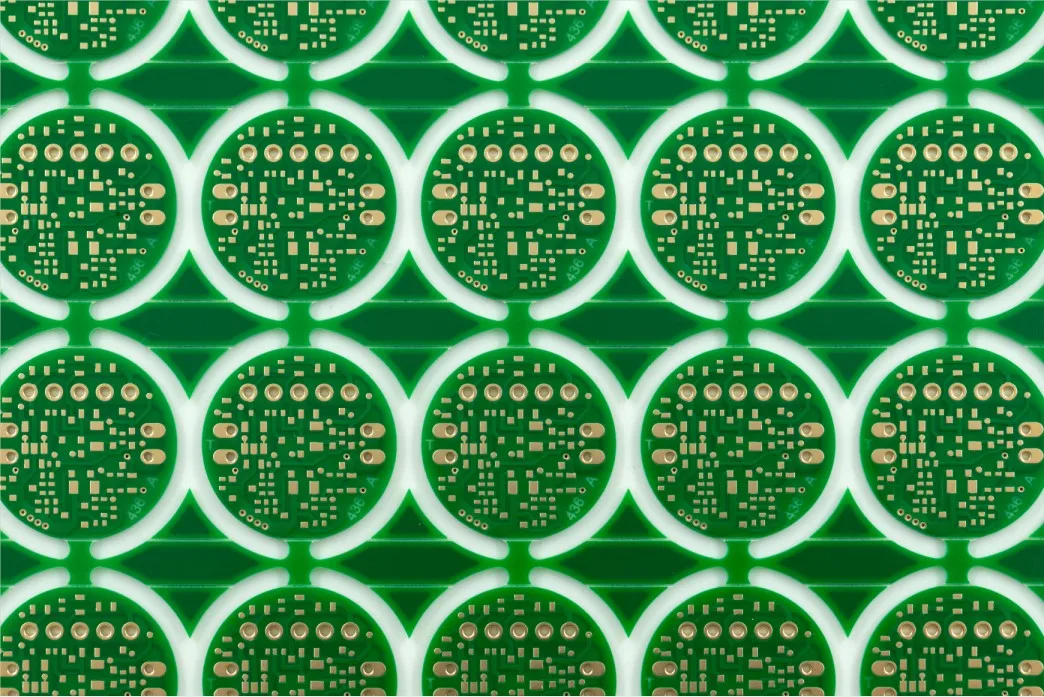
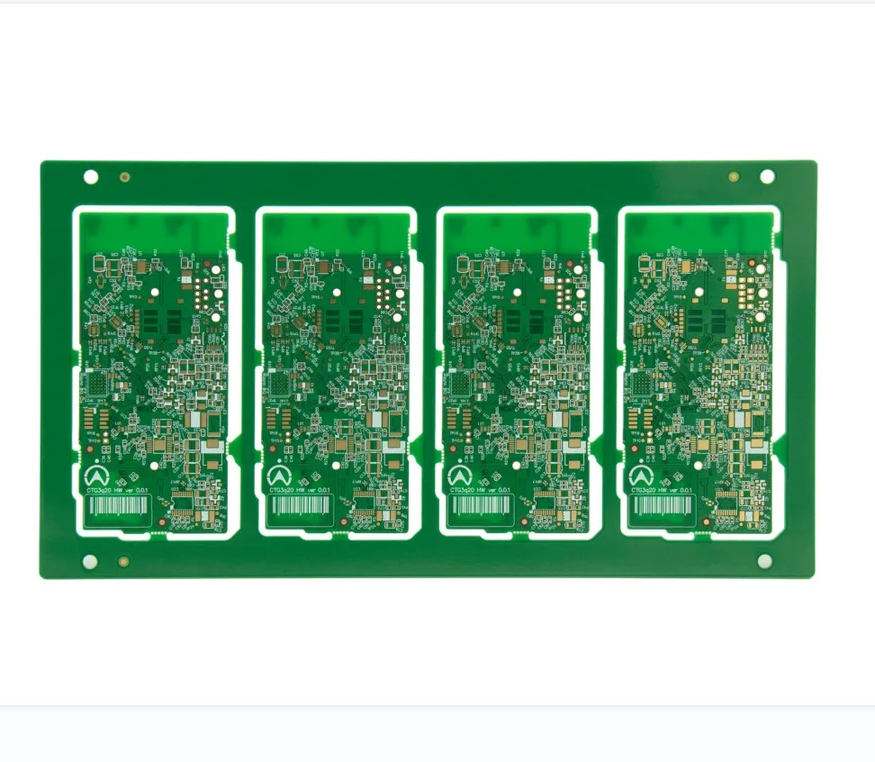
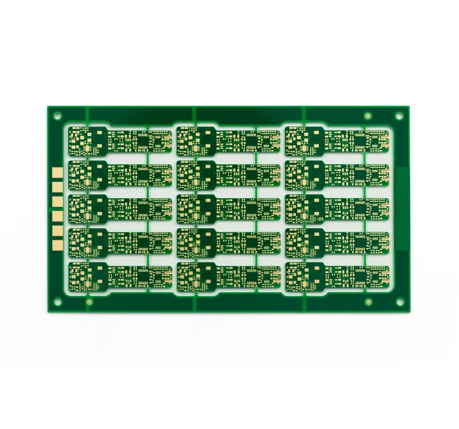
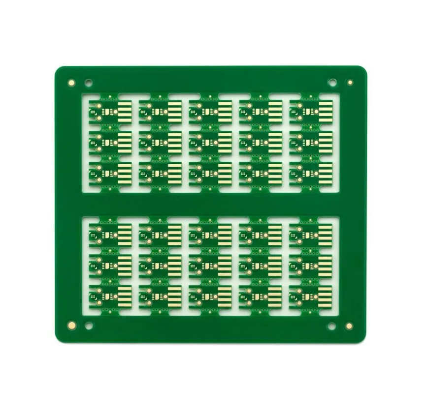
JINHUA manufacturer blind hole wholesale hdi multilayer pcb
- Category: PCB & PCBA >>>
- Supplier: Jinhua Technology (shenzhen) Co. Ltd.
Share on (1600603118849):
Product Overview
Description
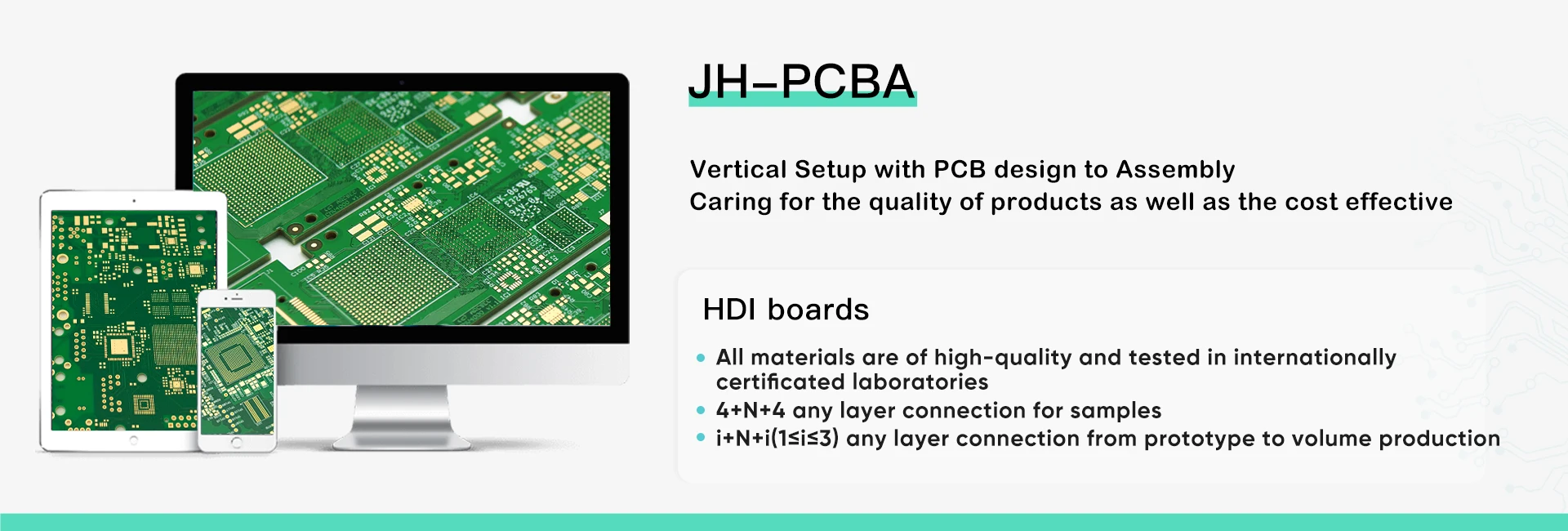
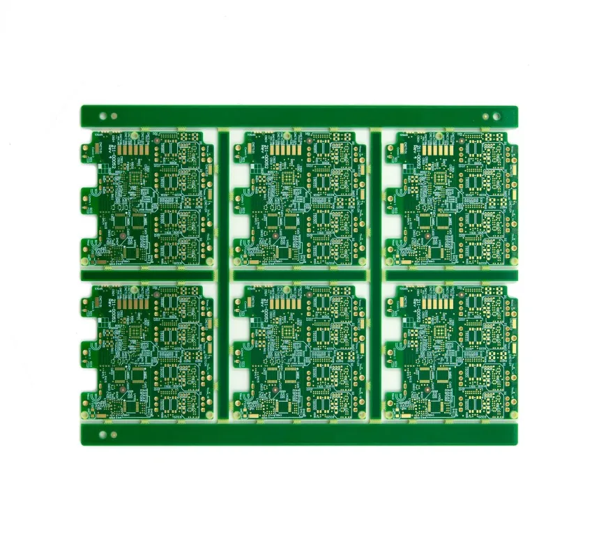
HDI means HIGH DENSITY INTERCONNECT PCBS. Owing to increase, density they provide the necessary routing solutions for large pin-count chips that are utilized in mobile devices and other high tech products.
What kinds of HDI board you can get from us?
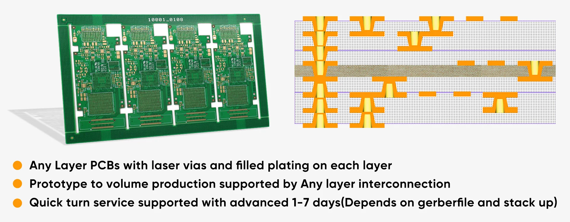
HDI PCBs have a much higher wiring and pad connection density than traditional PCBs, due to their design constraint. The structural build up is explained below.
1+N+1 – PCBs contain 1 “build-up” of high-density interconnection layers.
i+N+i (i ≥ 2) – PCBs contain 2 or more “build-up” of high density interconnection layers. Microvias on different layers can either be staggered or stacked up.
Any Layer HDI – The layers of a PCB are high density interconnection layers which allow the conductors on any layer of the PCB to be interconnected freely with copper filled stacked microvia structures.
Applications of the HDI PCBs:
· Automotive Industries: Engine Control Units, GPS, Dashboard Electronics.
· Telecom Industries: Computers, Laptops, Tablets, Wearable Electronics, Internet of Things
· Military: Military Routers, COTS Boards, etc.
· Medical: 35 Micron trace space board, Pacemakers
· Semiconductors: MCM / Flip Chip / Wirebond, stacked microvias
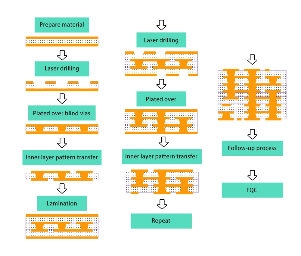
HDI Production Procress:
Product Description
| Process Capability of HDI PCB | ||
| Items | Content | Production Capability |
| 1 | Number of Layers | 4-22 layers standard, 30 layers advanced |
| 2 | Material | FR4 standard, FR4 high performance, Halogen free FR4, Rogers |
| 3 | Copper finished | 18um-70um |
| 4 | Min.track and gap | 0.075mm/0.075mm |
| 5 | PCB thickness | 0.4mm-6.0mm |
| 6 | Max dimensions | 610mm*450mm, depends on the laser drilling mechine |
| 7 | Surface treatment | OSP, ENIG, Immersion Tin, Immersion Silver, Electrolytic Gold, Gold fingers |
| 8 | Min. Mechanical Drill | 0.15mm |
| 9 | Min. Laser Drill | 0.1mm standard, 0.075mm advanced |
| 10 | Quality Standard | IPC-600,6012, Class II amd III |
| 11 | HDI Technology | 4+N+4, 4 step any layer connection |
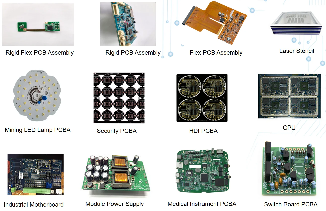
Related Products
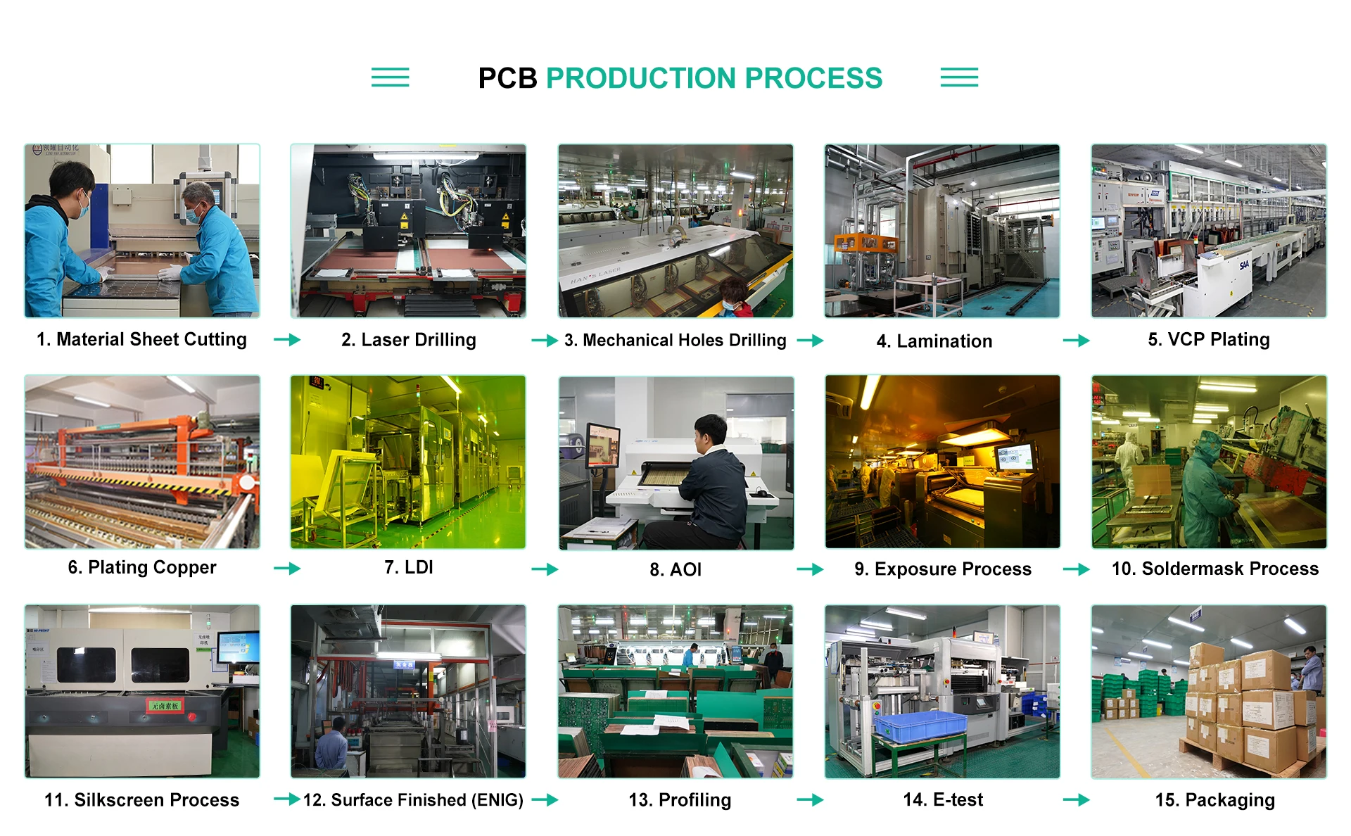
Production Process
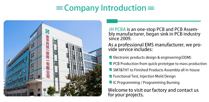
Company Information
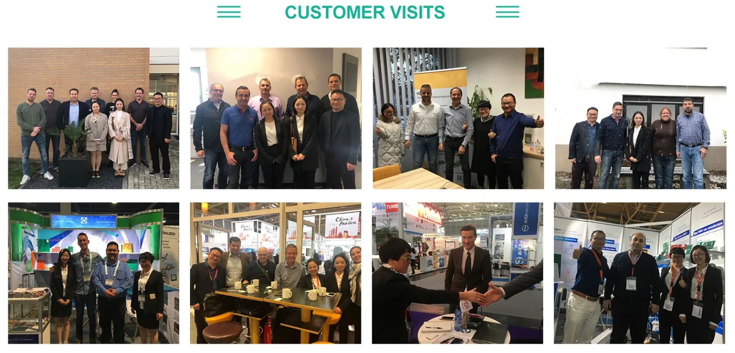
Exhibition
Packaging
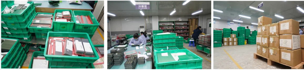
Bubble package, EPE package, ESD Bag,Vacuum bag
FAQ
Q1. What does Jinhua Tecenology can do?
We can support you PCB Design, PCB board manufacturing, Components or Parts Source, Surface Mount (SMT), Thru-Hole (THT),hybrid of both, Functional Test, Wire Soldering etc one stop PCB&PCBA service
Q2. For PCB quotation, what files format do JINHUA need?
Gerber, Protel 99SE, DXP, PADS 9.5, AUTOCAD, CAM350 are OK.
| Bare PCB Prototype | |
| Layer | Quick Turn |
| 2 | 24 hours |
| 4 | 48 hours |
| 6-8 | 72 hours |
Q3. What will I get from you? Are my files safe?
You will get the free DFM feedback for PCB gerber files, BOM list components feedback, Quotation feedback within 2 hours. NDA can be signed for extra security issue.
Q4. MOQ?
There is no MOQ in Jinhua Tecenology. We can offer prototype, expedite prototype, small&medium amount, big amount pcb & pcba service.
We Recommend


New Arrivals
New products from manufacturers at wholesale prices