
Китайский производитель печатных плат обеспечивает сборку печатных плат
- Category: PCB & PCBA >>>
- Supplier: Shenzhen Dyc Electronic Technology Co. Ltd.
Share on (62503548447):
Product Overview
Description

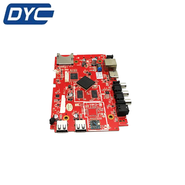
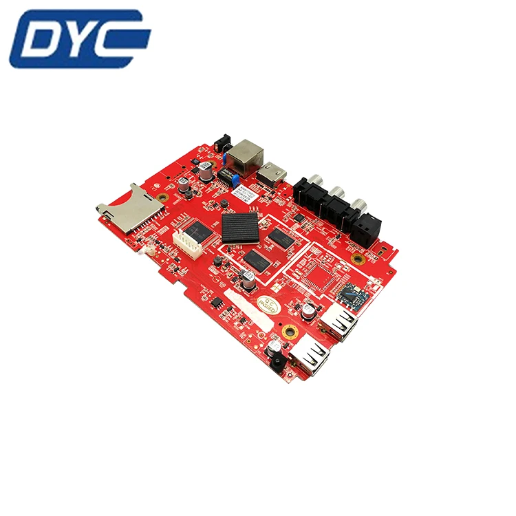
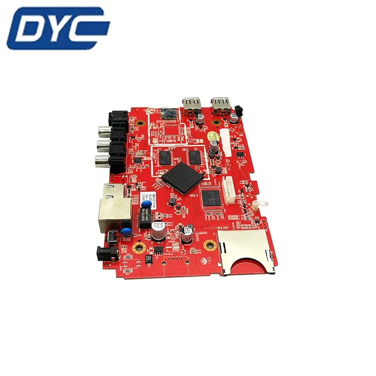
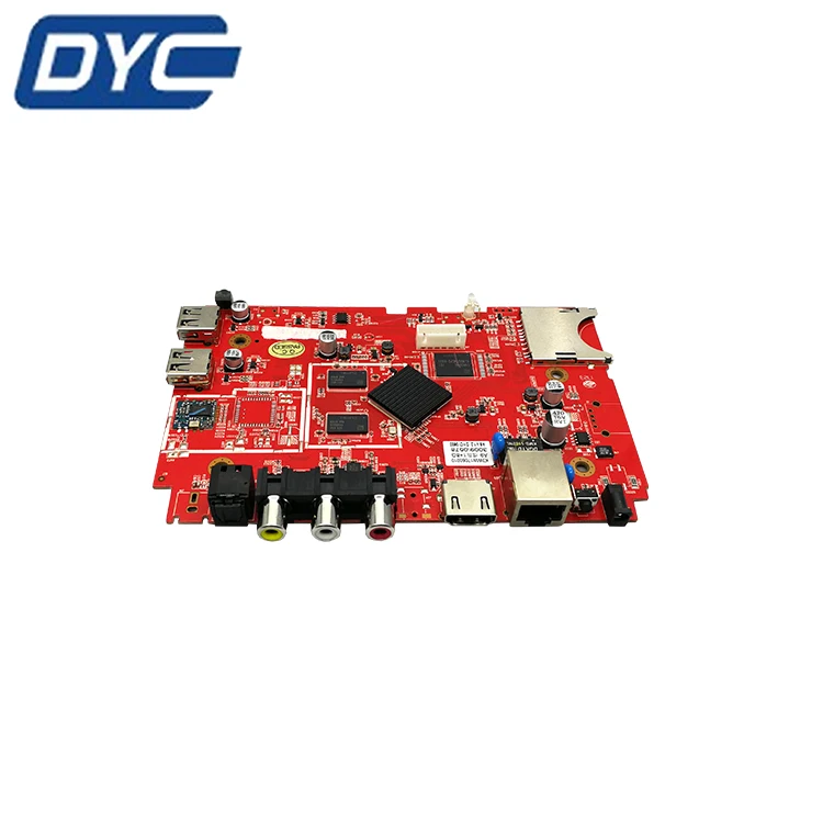
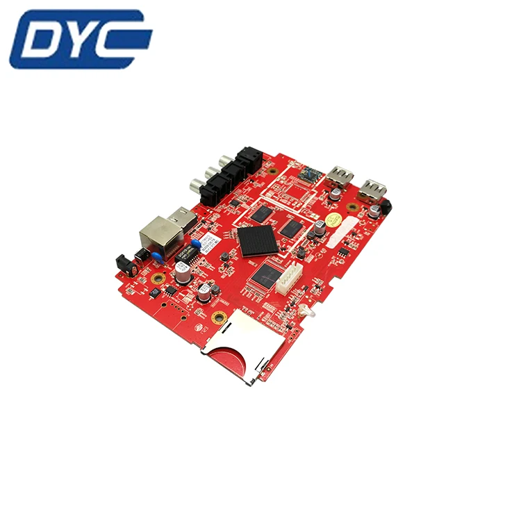
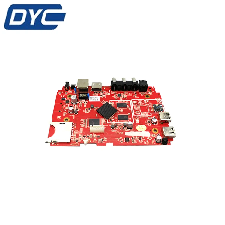
China pcb manufacturer provide printed circuit board pcb assembly fabrication
Our Services
1. PCB design ,PCB clone and copy ,ODM PCBA service.
2. Schematic design and Layout
3. Fast PCB&PCBA prototype and Mass Production
4. Electronic Components Sourcing Services
5. PCB Assembly Services:SMT,DIP&THT,BGA repair and reballing
6. ICT, Constant Temperature Burn-in and Function Test
7. Stencil,Cables and Enclosure building
8. Standard Packing and On time Delivery
Product Description
PCBA Capability
Layer:1~30 layers
Materials: FR-4, CEM-3, Teflon, Aluminum, Rogers, High Tg
Surface finished:Lead Free HASL,Immersion Gold/Tin/Silver, OSP, Gold Finger Plating, Selective Immersion Gold,Gold Plating
| PCB Assembly Manufacturing | Available PCB Assembly Services | PCB Assembly Machines |
| 5 SMT lines | Up to 12 layers, blind and buried via, impedance, heavy copper, HDI. | YAMAHA YS12F series SMT |
| mounters | ||
| 2 DIP lines | SMT/DIP | Auto solder paste screen printer |
| 0201 component | In circuit test | Reflow ovens with 10 zones |
| 0.25mm BGA | Function circuit test | Auto optical inspection |
| SMT 5 million spot daily | Burn in test | Wave soldering (lead-free) |
| DIP 1 million spot daily | Box Building | PCB assembly test room |
PCB Capability
| English | Metric | |||
| 1 | Max. Pamnel Size | 22" x 26" | 550 x 650m | |
| 2 | Mechanical Drill | |||
| Min. Finished Holes Size | 0.004" | 0.10mm | ||
| Finished Holes Tolerance | PTH | ±0.003" | ±0.075mm | |
| NPTH | ±0.002" | ±0.050mm | ||
| Press Fit | ±0.002" | ±0.050mm | ||
| Aspect Ratio | 9:01 | 9:01 | ||
| 3 | Laser Drill | |||
| Microvias diameter | 0.004" - 0.006" | 0.10 - 0.15mm | ||
| Aspect Ratio | 1:01 | 1:01 | ||
| 4 | Min. Line Width/Spacing | ½oz / 18um | 0.003" / 0.003" | 0.075 / 0.075mm |
| 1oz / 35um | 0.006" / 0.006" | 0.15 / 0.15mm | ||
| 2oz / 70um | 0.008" / 0.008" | 0.20 / 0.20mm | ||
| 3oz / 105um | 0.010" / 0.010" | 0.25 / 0.25mm | ||
| 5 | Registration | |||
| Solder Mask | ±0.003" | ±0.075mm | ||
| Layer to Layer | ±0.0024" | ±0.060mm | ||
| Copper Feature to Holes(Outer) | ±0.003" | ±0.075mm | ||
| Min. Plated Drills to Copper (inner) | 2L - 8L | 0.010" | 0.25mm | |
| 10L -30L | 0.012" | 0.30mm | ||
| 6 | Board Outline | |||
| Edge to Edge Tolerance | ±0.004" | ±0.10mm | ||
| Holes to Edge Tolerance | ±0.004" | ±0.100mm | ||
| Min. Copper to Edge distance | Outer | 0.010" | 0.25mm | |
| Inner | 0.016" | 0.40mm | ||
| 7 | Max. Copper Thickness | 4oz | 140μm | |
| 8 | Max. Board Thickness | 0.189" | 4.80 mm | |
| 9 | Min Board Thickness | 2L | 0.008" | 0.20mm |
| 4L | 0.016" | 0.40mm | ||
| 6L -30L | 0.020" | 0.60mm | ||
| 10 | Min. Core Thickness | 0.004" | 0.10mm | |
| 11 | Min. Soldermask Dam | 0.004" | 0.10mm | |
| 12 | Controlled Impedance (Ohm) | ±7% - 10% | ±7% - 10% | |
Production Flow Chat


Certifications

Buyer Feedback

FAQ
Q1: What should i provide to get one PCB quotation?
A1: Gerber file, PCB technical, quantity.
( Layer, Base material, Finished copper, Finished thickness, Surface finish, Solder mask)
Q2: What file formats of PCB do you support?
A2: Gerber file, PADS_LOGIC, AD, protel, allegro, Orcad.
Q3: Will you check the PCB gerber file before production?
A3: Yes, our engineer will check the coordinate file, layout, silkscreen, packing and full design to avoid the design-error.
Q4: My budget is limited, can you provide solutions to save cost ?
A4: Yes, we can. For example:
a, Replace the DIP components with SMD components, so it can narrow the PCB board size to save cost.
b, Relayout the pcb to reduce the size, it can save cost.
c, we can recommend you suitablet PCB tecnical parameter according to the product character, like board materials, thickness etc.
Q5: Do you have any other special discount ?
A5: Yes, we provide free panel, free test and free packaging.
Any other questions please contact us directly. As a global supplier of PCB /PCBA,we will meet the needs of customers world wide,with professional technology and sincere spirit of service and reasonable price, delivery on time. We look forward to your visit and establish long-term cooperation.
====> www.dyc-pcba.en.alibaba.com
Contact Us

We Recommend


New Arrivals
New products from manufacturers at wholesale prices


